 ALLPCB


If you're diving into PCB design or manufacturing, understanding the different types of holes in a printed circuit board (PCB) is essential. So, what are the main PCB hole types? They include thru-hole, blind vias, buried vias, microvias, plated through holes, and non-plated through holes. Each type serves a unique purpose, such as electrical interconnections or component mounting, and choosing the right one can make or break your design's performance and cost. In this comprehensive guide, we'll break down these hole types, explain their uses, and help you make informed decisions for your next project.
Introduction to PCB Hole Types
Printed circuit boards are the backbone of modern electronics, connecting components and enabling functionality in devices from smartphones to industrial machinery. A key feature of any PCB is its holes, also known as vias or drill holes, which facilitate electrical interconnections between layers or provide space for component mounting. These holes come in various forms, each with specific applications, manufacturing processes, and design considerations.
Whether you're working on a simple single-layer board or a complex multilayer design, knowing the differences between thru-hole, blind vias, buried vias, and other types like microvias can optimize your PCB for performance, reliability, and cost. In this blog, we'll explore each type in detail, focusing on long-tail keywords like "drill hole of PCB," "plated through holes," "non-plated through holes," "microvias," "electrical interconnections," and "component mounting" to ensure you have all the information you need.
Why PCB Hole Types Matter in Design and Manufacturing
The type of hole you choose for your PCB directly impacts signal integrity, manufacturing complexity, and overall cost. For instance, a simple thru-hole might be ideal for mounting large components like capacitors, while microvias are better suited for high-density interconnect (HDI) designs where space is limited. Using the wrong hole type can lead to issues like poor electrical connections, increased impedance, or even board failure under stress.
Additionally, the manufacturing process varies for each hole type. Some, like plated through holes, require additional steps such as electroplating to ensure conductivity, while others, like non-plated through holes, are purely mechanical and simpler to produce. Understanding these differences helps you balance design needs with production costs.
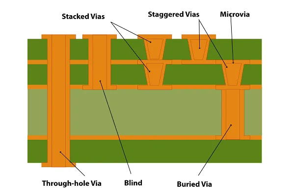
Thru-Hole: The Classic Choice for Component Mounting
Thru-hole, also known as through-hole, is one of the most common and oldest types of PCB holes. These holes extend through the entire thickness of the board, from the top layer to the bottom layer. They are primarily used for component mounting, especially for larger components like resistors, capacitors, and connectors that require a strong mechanical bond.
Thru-holes are typically drilled using a mechanical drill, with diameters ranging from 0.2 mm to several millimeters, depending on the component leads they need to accommodate. After drilling, these holes are often plated with a conductive material like copper to create plated through holes (PTH), ensuring electrical interconnections between layers. For example, a typical plated thru-hole might have a copper thickness of 25 micrometers (1 mil) to handle currents up to 5 amps without overheating.
However, not all thru-holes are plated. Non-plated through holes (NPTH) are used for mechanical purposes, such as mounting screws or alignment pins, where no electrical connection is needed. These are simpler to manufacture since they skip the plating step, reducing costs.
Key Benefits of Thru-Hole:
- Strong mechanical support for larger components.
- Reliable electrical interconnections for multilayer boards when plated.
- Easy to inspect and repair during assembly.
Drawbacks:
- Takes up more space, limiting design density.
- Not ideal for high-speed signals due to potential impedance mismatches (e.g., above 50 ohms in some designs).
Blind Vias: Connecting Surface to Inner Layers
Unlike thru-holes, blind vias do not pass through the entire PCB. Instead, they connect the outer layer (top or bottom) to one or more inner layers, stopping at a specific depth. This makes them ideal for high-density designs where space on the opposite side of the board needs to remain free for other components or traces.
Blind vias are often used in multilayer PCBs to create electrical interconnections without cluttering the opposite surface. They are typically formed using controlled-depth drilling or laser drilling, especially in HDI boards. For instance, a blind via might have a diameter of 0.15 mm and a depth of 0.3 mm to connect the top layer to the second layer of a 6-layer PCB.
Key Benefits of Blind Vias:
- Saves space on the opposite side of the PCB.
- Supports high-density layouts for compact devices.
- Reduces signal interference by shortening connection paths, often maintaining signal integrity at speeds up to 10 Gbps.
Drawbacks:
- More expensive to manufacture due to precise drilling requirements.
- Difficult to inspect or repair once the board is assembled.
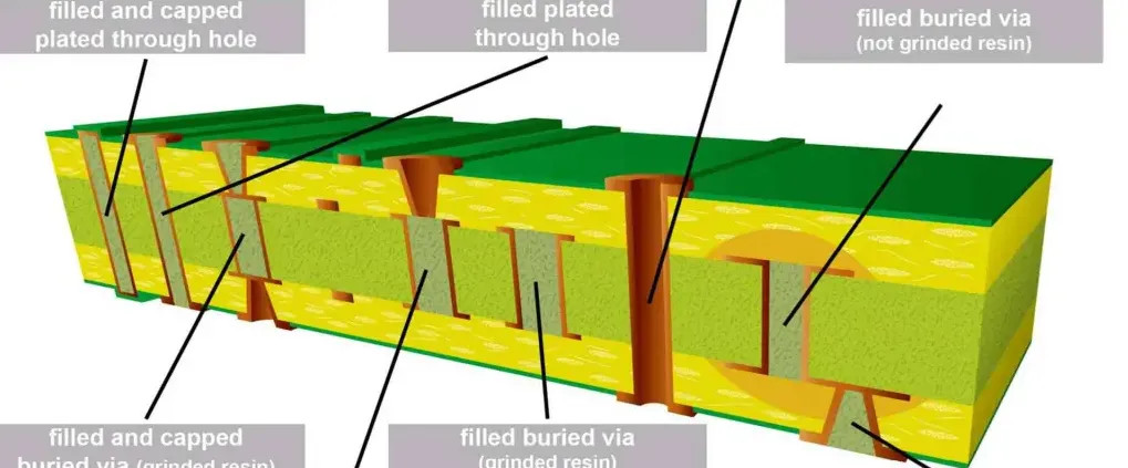
Buried Vias: Hidden Connections Between Inner Layers
Buried vias are similar to blind vias but are entirely hidden within the PCB. They connect two or more inner layers without reaching the outer surfaces (top or bottom). Because they don't appear on the surface, buried vias are perfect for maximizing space on both sides of the board, making them a popular choice in complex multilayer designs.
These vias are typically created during the lamination process of multilayer PCBs, before the outer layers are added. Like blind vias, they require precise manufacturing techniques, often increasing production costs. A typical buried via might span layers 2 to 4 in an 8-layer PCB, with a diameter as small as 0.1 mm in advanced designs.
Key Benefits of Buried Vias:
- Frees up space on both outer layers for components or traces.
- Enhances signal integrity by reducing trace lengths, often critical for frequencies above 1 GHz.
- Supports dense routing in multilayer boards.
Drawbacks:
- High manufacturing cost due to complex lamination and drilling processes.
- Impossible to access or repair after board assembly.
Microvias: Tiny Holes for High-Density Designs
Microvias are extremely small vias, typically with diameters less than 0.15 mm, used in high-density interconnect (HDI) PCBs. They are often created using laser drilling rather than mechanical drilling due to their small size and precision requirements. Microvias are essential for modern electronics like smartphones and wearables, where space is at a premium.
These vias can be blind or buried and are primarily used for electrical interconnections in multilayer boards. Their small size allows for tighter routing, enabling designers to pack more functionality into smaller areas. For example, a microvia might connect layers in a 12-layer PCB with a depth-to-diameter ratio (aspect ratio) of 1:1 to ensure reliability.
Key Benefits of Microvias:
- Enables ultra-compact designs with high component density.
- Improves signal integrity for high-speed applications (e.g., supporting data rates up to 25 Gbps).
- Reduces parasitic capacitance and inductance compared to larger vias.
Drawbacks:
- Expensive to produce due to laser drilling and precise manufacturing.
- Limited current-carrying capacity due to small size, often below 1 amp.
Plated Through Holes vs. Non-Plated Through Holes
When discussing the drill hole of PCB, it's important to distinguish between plated through holes (PTH) and non-plated through holes (NPTH). Both are types of thru-holes, but their purposes differ significantly.
Plated Through Holes (PTH): These holes are coated with a conductive material, usually copper, to create electrical interconnections between layers. PTHs are crucial for multilayer PCBs, allowing signals and power to travel through the board. The plating process typically adds a layer of copper about 20-30 micrometers thick, ensuring durability and conductivity for currents up to several amps.
Non-Plated Through Holes (NPTH): These holes lack any conductive coating and are used solely for mechanical purposes. They might serve as mounting holes for screws or as alignment guides during assembly. Since there's no plating, NPTHs are cheaper and faster to produce but offer no electrical functionality.
Comparison:
- PTHs are essential for electrical interconnections and component mounting in multilayer designs.
- NPTHs are ideal for mechanical support without adding unnecessary cost.
Applications of PCB Hole Types in Electrical Interconnections and Component Mounting
Each PCB hole type plays a critical role in either electrical interconnections or component mounting, often serving both purposes depending on the design.
Electrical Interconnections: Vias like blind, buried, and microvias are primarily used to connect traces between layers, ensuring signals and power are routed efficiently. For high-speed designs, minimizing via size (e.g., using microvias) reduces signal delay and impedance, critical for maintaining performance at frequencies above 500 MHz.
Component Mounting: Thru-holes, especially plated ones, are the go-to choice for mounting through-hole components. Their larger size provides a secure mechanical connection, which is vital for components subject to vibration or thermal stress, such as connectors in industrial equipment.
Understanding the balance between these applications helps designers choose the right hole type. For instance, a mixed-signal PCB might use microvias for high-speed digital signals on inner layers while relying on thru-holes for mounting analog components on the surface.
Design Considerations for Choosing the Right Hole Type
Selecting the appropriate hole type for your PCB involves several factors:
- Board Complexity: Multilayer boards often require blind or buried vias to manage dense routing, while single-layer boards can rely on thru-holes.
- Signal Speed: High-speed signals benefit from smaller vias like microvias to reduce inductance, often keeping values below 1 nH.
- Cost: Thru-holes and NPTHs are more cost-effective, while blind, buried, and microvias increase manufacturing expenses due to precision requirements.
- Space Constraints: HDI designs favor microvias and buried vias to maximize usable space on outer layers.
By weighing these factors, you can optimize your PCB design for both performance and budget. For example, a consumer electronics product might prioritize microvias for compactness, while an industrial control board might use thru-holes for durability.
Manufacturing Insights: Drilling and Plating Processes
The drill hole of PCB is a critical manufacturing step that varies by hole type. Mechanical drilling is used for larger holes like thru-holes, with drill bits ranging from 0.2 mm to 6 mm in diameter. Laser drilling, on the other hand, is employed for microvias, achieving precision down to 0.05 mm for HDI boards.
Plating, used for PTHs and most vias, involves depositing a conductive layer inside the hole. This process, often done via electroplating, ensures reliable electrical interconnections. The thickness of the plating can affect performance; for instance, a 25-micrometer copper layer is standard for most applications, but high-current designs might require up to 50 micrometers.
Non-plated through holes skip this step, saving time and cost but limiting their use to mechanical functions. Understanding these processes helps designers communicate effectively with manufacturers to avoid production delays or defects.
Conclusion: Making Informed Choices for PCB Hole Types
From thru-hole to blind vias, buried vias, and microvias, each PCB hole type offers unique advantages for electrical interconnections and component mounting. Thru-holes provide robust mechanical support, while blind and buried vias save space in multilayer designs. Microvias enable high-density layouts for cutting-edge electronics, and the choice between plated and non-plated through holes can impact both functionality and cost.
By understanding the strengths and limitations of each type, as well as key design considerations like signal speed and board complexity, you can create PCBs that meet your project's specific needs. Whether you're optimizing for performance, compactness, or budget, the right drill hole of PCB can elevate your design to the next level.
Armed with this knowledge, you're better equipped to tackle your next PCB project with confidence. Keep these insights in mind as you navigate the intricate world of PCB design and manufacturing.


