 ALLPCB


In the fast-evolving world of electronics, understanding 4 Layer PCB Stack-up Technology is crucial for engineers and designers aiming to create high-performance, reliable, and efficient circuit boards. Whether you're working on compact devices or complex systems, a well-designed 4 Layer PCB stack-up can make all the difference in signal integrity, thermal management, and overall functionality. This technology is especially vital when considering aspects like design for airflow and multilayer PCBs board configurations. In this comprehensive guide, we'll dive deep into why knowing 4 Layer PCB Stack-up Technology is essential and how it impacts your projects.
What Is 4 Layer PCB Stack-up Technology?
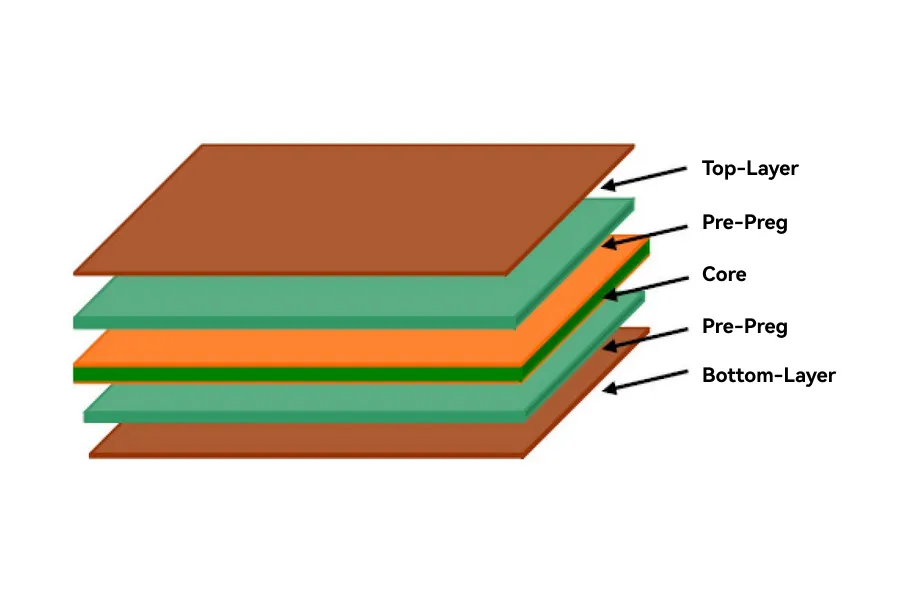
A 4 Layer PCB Stack-up refers to the arrangement of conductive and insulating layers in a printed circuit board (PCB) that consists of four distinct layers of copper. These layers are typically organized to include two outer layers for signal routing or components and two inner layers often dedicated to power and ground planes. This setup is bonded together with insulating materials like prepreg and core, ensuring electrical isolation and structural integrity.
Unlike single or double-layer boards, a 4 Layer PCB offers more routing space and better control over signal integrity, making it a popular choice for modern electronics with higher complexity. Understanding this technology is key to optimizing design for airflow, managing electromagnetic interference (EMI), and ensuring efficient power distribution in multilayer PCBs board designs.
Why Is 4 Layer PCB Stack-up Technology Important?
The importance of 4 Layer PCB Stack-up Technology lies in its ability to address the challenges of modern electronic designs. As devices become smaller and more powerful, the need for efficient space usage, reduced noise, and reliable performance grows. Here's why you need to know about this technology:
- Enhanced Signal Integrity: With dedicated power and ground planes in the inner layers, a 4 Layer PCB minimizes signal crosstalk and noise, ensuring cleaner and faster signal transmission. For high-speed designs, this can mean achieving signal speeds up to 5 Gbps or higher with controlled impedance, often targeted at 50 ohms for many applications.
- Compact Design: Multilayer PCBs board configurations like the 4 Layer stack-up allow for more components and routing in a smaller footprint, ideal for compact devices like smartphones or IoT gadgets.
- Better Power Distribution: Inner layers dedicated to power and ground provide a low-impedance path for current, reducing voltage drops and improving power delivery to components.
- EMI Reduction: The close proximity of power and ground planes in a 4 Layer PCB acts as a natural shield, reducing electromagnetic interference, which is critical for sensitive applications.
By mastering 4 Layer PCB Stack-up Technology, designers can tackle these challenges head-on, ensuring their products meet performance and reliability standards.
How Does 4 Layer PCB Stack-up Impact Design for Airflow?
When designing electronic devices, thermal management is a critical factor, and 4 Layer PCB Stack-up Technology plays a significant role in optimizing design for airflow. Poor heat dissipation can lead to component failure, reduced lifespan, and performance issues. Here's how a well-planned 4 Layer stack-up helps:
- Thermal Distribution: The inner power and ground planes in a 4 Layer PCB can act as heat spreaders, distributing heat more evenly across the board. This prevents hot spots that could damage components.
- Component Placement Flexibility: With more layers for routing, designers can strategically place heat-generating components on outer layers where airflow from fans or vents can cool them more effectively. For instance, placing high-power ICs on the top layer near a cooling vent can reduce temperatures by up to 10-15°C compared to cramped single-layer designs.
- Reduced Board Thickness: A 4 Layer PCB stack-up, often ranging from 0.8mm to 1.6mm in total thickness, allows for thinner boards compared to stacking multiple single-layer boards, improving airflow around and through the device enclosure.
Designing for airflow with a 4 Layer PCB stack-up means considering both the physical layout and the material properties, such as using thermal vias to transfer heat to inner layers or external heat sinks. This approach ensures that your multilayer PCBs board remains cool under heavy operation.
Key Benefits of 4 Layer PCB Stack-up in Multilayer PCBs Board Designs
Multilayer PCBs board designs, particularly those using a 4 Layer stack-up, offer several advantages that make them indispensable for complex electronics. Let's explore these benefits in detail:
1. Improved Routing Density
With four layers available, designers have more room to route traces without overcrowding. This is especially useful for high-density interconnect HDI PCB designs where space is limited. For example, a typical 4 Layer PCB can accommodate up to 30% more traces per square inch compared to a double-layer board.
2. Controlled Impedance for High-Speed Signals
In high-speed applications, maintaining consistent impedance is vital for signal integrity. A 4 Layer PCB stack-up allows designers to control impedance by adjusting the distance between signal layers and ground planes, often targeting values like 50 ohms or 75 ohms for specific applications like USB or HDMI interfaces.
3. Reduced Manufacturing Costs Compared to Higher Layer Counts
While a 4 Layer PCB is more expensive than a 2 Layer board, it strikes a cost-effective balance for many projects compared to 6 or 8 Layer boards. The 4 layer PCB manufacturing cost might be around 20-30% higher than a 2 Layer board but significantly less than higher layer counts, making it a practical choice for medium-complexity designs.
4. Scalability for Future Upgrades
A 4 Layer PCB stack-up provides enough flexibility to accommodate future design changes or additional features without requiring a complete redesign. This scalability is a major advantage for iterative product development in multilayer PCBs board projects.
Best Practices for Designing a 4 Layer PCB Stack-up
To fully leverage 4 Layer PCB Stack-up Technology, follow these best practices to ensure optimal performance in your multilayer PCBs board designs:
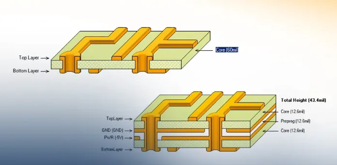
- Standard Layer Arrangement: Use a common stack-up configuration like Signal-Power-Ground-Signal. This setup places power and ground planes in the middle to reduce noise and improve signal integrity on the outer layers.
- Minimize Via Usage: Excessive vias can increase manufacturing costs and introduce signal delays. Plan your routing to keep vias to a minimum, ideally below 100 per square inch for cost efficiency.
- Balance Copper Thickness: Ensure uniform copper thickness across layers, typically 1 oz (35 μm) for outer layers and 0.5-1 oz for inner planes, to avoid warping during manufacturing.
- Incorporate Thermal Management: As part of your design for airflow, add thermal vias near high-power components to transfer heat to inner layers or external heat sinks. Space these vias at intervals of about 0.3mm for effective heat dissipation.
- Test for Signal Integrity: Use simulation tools to verify impedance and signal performance before finalizing your design. Aim for a signal return path that minimizes loop area to reduce EMI.
By adhering to these practices, you can create robust and efficient 4 Layer PCB designs that meet the demands of modern electronics.
Suggested Reading: Optimizing 4-Layer PCB Layer Stackup: A Practical Guide
Common Challenges in 4 Layer PCB Stack-up and How to Overcome Them
While 4 Layer PCB Stack-up Technology offers many benefits, it also comes with challenges that designers must address to ensure success in multilayer PCBs board projects.
1. Signal Crosstalk
Challenge: Close proximity of traces on different layers can lead to crosstalk, especially in high-speed designs.
Solution: Maintain adequate spacing between signal traces (at least 3 times the trace width) and ensure ground planes are continuous without splits to provide a proper return path.
2. Thermal Issues
Challenge: Heat buildup in compact designs can affect performance, even with a focus on design for airflow.
Solution: Use thermal vias and ensure proper placement of heat-generating components near cooling mechanisms. Consider materials with higher thermal conductivity if heat dissipation remains a concern.
3. Manufacturing Complexity
Challenge: A 4 Layer PCB requires precise alignment and lamination, increasing the risk of manufacturing defects.
Solution: Work closely with your fabrication partner to define clear design rules, such as minimum trace widths (typically 6 mil) and spacing, to avoid production issues.
Applications of 4 Layer PCB Stack-up Technology
The versatility of 4 Layer PCB Stack-up Technology makes it suitable for a wide range of applications, particularly in industries requiring reliable multilayer PCBs board designs. Some common uses include:
- Consumer Electronics: Smartphones, tablets, and wearables often use 4 Layer PCBs to fit complex circuitry into small spaces while maintaining performance.
- Automotive Systems: Control units and sensors in vehicles rely on 4 Layer stack-ups for robust signal integrity and power management under harsh conditions.
- Industrial Equipment: Machinery control boards benefit from the EMI reduction and PCB thermal management offered by 4 Layer designs.
- Medical Devices: Portable diagnostic tools and monitoring systems use 4 Layer PCBs for compact, reliable designs that prioritize signal accuracy.
These applications highlight the importance of understanding 4 Layer PCB Stack-up Technology to meet industry-specific requirements effectively.
Suggested Reading: 4 layers PCB: Everything You Need to Know
Conclusion: Mastering 4 Layer PCB Stack-up Technology for Success
In today's electronics landscape, knowing 4 Layer PCB Stack-up Technology is not just an advantage—it's a necessity. From enhancing signal integrity and power distribution to optimizing design for airflow, this technology empowers designers to create high-performing, reliable multilayer PCBs board solutions. By understanding the benefits, best practices, and potential challenges, you can confidently tackle complex projects and deliver products that meet modern standards.
Whether you're working on consumer gadgets, automotive systems, or industrial applications, a well-designed 4 Layer PCB stack-up can significantly impact your project's success. Take the time to plan your layer arrangement, prioritize thermal management, and simulate performance to ensure your designs stand out in a competitive market. With the right knowledge and approach, 4 Layer PCB Stack-up Technology becomes a powerful tool in your engineering toolkit.


