 ALLPCB


If you're looking for a reliable way to cool your PCB and prevent overheating, thermal vias are a key solution. These small, strategically placed holes help transfer heat away from critical components, ensuring your board runs smoothly. In this guide, let's be with ALLPCB to dive deep into thermal via placement, covering everything from spacing and location optimization to preventing PCB hotspots. Whether you're a seasoned engineer or just starting, this thermal via placement guide will equip you with actionable tips for effective PCB component cooling.
Why Thermal Vias Matter for PCB Cooling
Modern electronic devices are packed with high-power components that generate significant heat. Without proper management, this heat can lead to performance issues, component failure, or even complete system breakdowns. Thermal vias act as a bridge, conducting heat from hot spots on the PCB surface to a heat sink or ground plane, where it can dissipate more effectively. By optimizing thermal via placement, you can enhance your board's reliability and lifespan.
Studies show that poor PCB thermal management can reduce component life by up to 50% for every 10°C rise in operating temperature above the recommended limit. This makes thermal vias not just a design choice but a necessity for high-performance boards.
Understanding Thermal Vias: The Basics
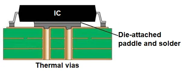
Thermal vias are small, plated-through holes in a PCB that facilitate heat transfer. Unlike regular vias used for electrical connections, their primary role is to move heat away from components like power ICs, LEDs, or processors. Typically, these vias are filled with conductive materials or left open, depending on the design needs, to maximize thermal conductivity.
The effectiveness of thermal vias depends on several factors, including their size, spacing, and placement. For instance, a via with a diameter of 0.3 mm can handle a certain amount of heat, but increasing the diameter to 0.5 mm can improve thermal conductivity by up to 30%, depending on the board's material and thickness.
How Thermal Vias Work
Thermal vias create a low-resistance path for heat to travel from a hot component to a cooler area, such as a copper plane or external heat sink. They work on the principle of thermal conductivity, where heat flows through materials with high conductivity (like copper) more easily than through insulators (like PCB material FR4 substrate). By placing thermal vias directly under or near heat-generating components, you can significantly reduce local temperatures.
Key Factors in Thermal Via Placement
Placing thermal vias effectively requires careful consideration of multiple design elements. Below, we explore the critical aspects of optimizing via location to ensure maximum cooling efficiency and prevent PCB hotspots.
1. Placement Under Heat-Generating Components
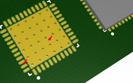
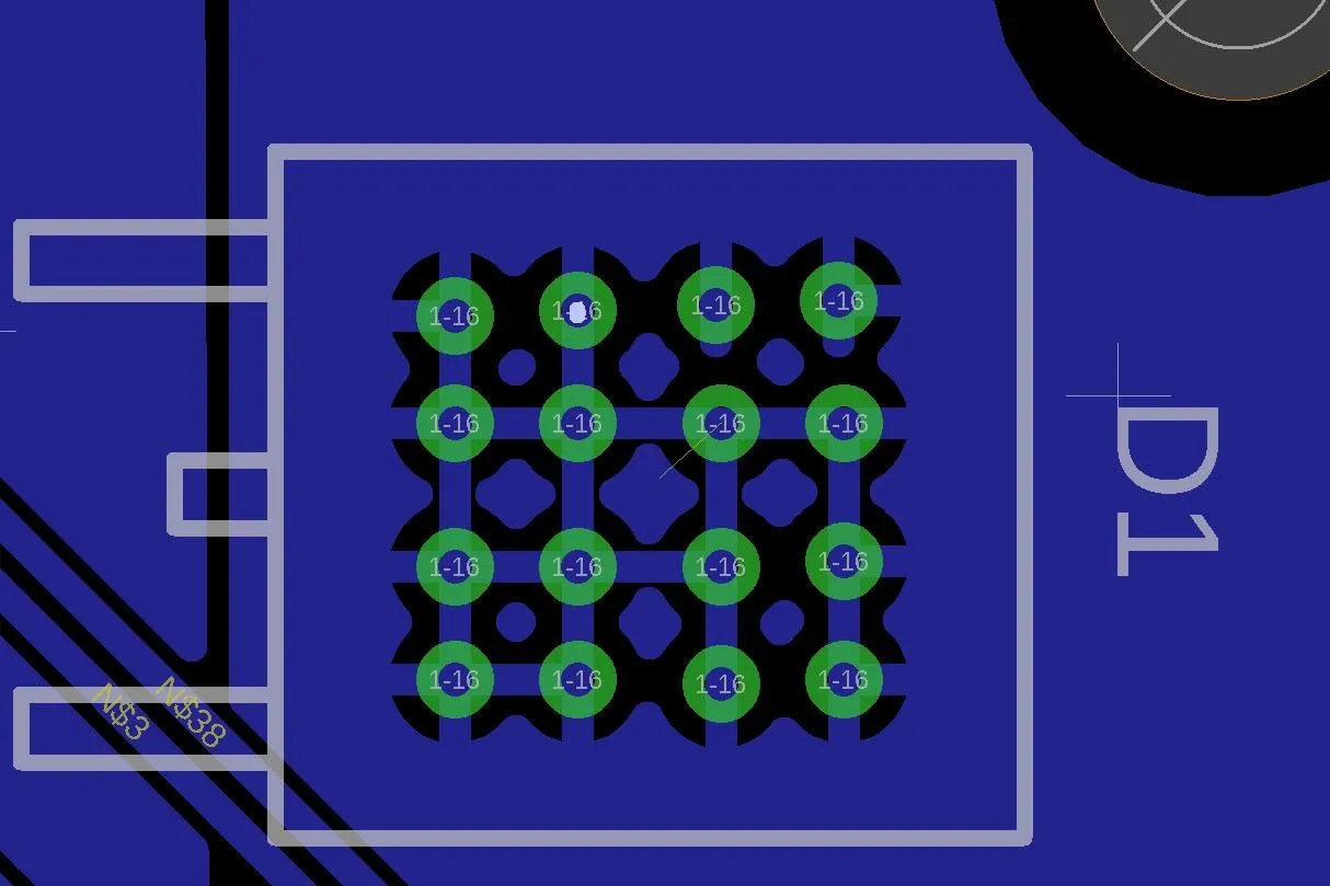
The most effective location for thermal vias is directly beneath components that generate the most heat, such as power transistors or microcontrollers. This minimizes the thermal resistance between the component and the heat-dissipating layer. For example, in a QFN package with a thermal pad, placing a grid of vias under the pad can reduce junction temperature by as much as 15°C, depending on the board layout.
Tip: Ensure that the vias connect to a large copper plane on the opposite side of the board or an internal layer for optimal heat spreading.
2. Thermal Via Spacing: Finding the Right Balance
Thermal via spacing is a critical factor in PCB component cooling. If vias are too close together, they can interfere with each other’s heat dissipation capacity and may cause manufacturing issues like solder wicking. If they’re too far apart, you lose efficiency in heat transfer. A general rule of thumb is to space vias at a distance of 1.2 to 1.5 times their diameter. For instance, for a 0.3 mm via, aim for a spacing of 0.36 to 0.45 mm.
However, this spacing can vary based on the component's heat output and board design. High-power components may require tighter spacing to handle greater heat loads, while standard designs can afford more relaxed spacing to ease manufacturing.
3. Number of Thermal Vias: More Isn’t Always Better
While it might seem logical to add as many thermal vias as possible, there’s a point of diminishing returns. Adding more vias beyond a certain number won’t significantly improve heat dissipation because the thermal resistance of the surrounding material becomes the limiting factor. Research suggests that 9 to 16 vias under a single thermal pad (for a typical 5x5 mm component) often strike the right balance between cooling and board space.
Tip: Use thermal simulation tools during the design phase to determine the optimal number of vias for your specific application.
4. Connection to Copper Planes or Heat Sinks
For thermal vias to work effectively, they must connect to a substantial copper area or heat sink. A large ground plane on an internal or bottom layer can act as a heat spreader, distributing heat evenly across the board. Without this connection, the vias will have limited impact. Ensure at least 1 to 2 square inches of copper area per high-power component for adequate heat dissipation.
Best Practices for Optimizing Via Location
Optimizing via location is about more than just placing them under components. It involves a holistic approach to high speed PCB layout to ensure heat is managed effectively across the entire board. Here are some best practices to follow:
- Avoid Blocking Airflow: Place vias in areas where they won’t obstruct airflow if your design relies on convection cooling. For forced-air systems, align vias with the direction of airflow for better heat removal.
- Minimize Thermal Resistance: Use shorter vias when possible by connecting to internal layers rather than routing heat through the entire board thickness. A via spanning only 0.8 mm of board thickness can have up to 20% lower thermal resistance than one spanning 1.6 mm.
- Balance Electrical and Thermal Needs: Avoid placing thermal vias too close to sensitive signal traces, as they can introduce noise or interference. Maintain a clearance of at least 0.5 mm from critical traces.
Preventing PCB Hotspots with Smart Design
PCB hotspots occur when heat concentrates in specific areas, often due to poor thermal management or uneven heat distribution. Preventing PCB hotspots starts with identifying potential problem areas during the design phase using thermal simulation software. Here’s how thermal vias can help:
- Distribute Heat Evenly: Place vias not just under components but also in areas surrounding high-heat zones to spread heat to cooler regions of the board.
- Use Multiple Via Arrays: For larger components or areas with intense heat generation, create multiple small arrays of vias rather than a single large cluster. This approach can reduce hotspot temperatures by up to 10°C in some designs.
- Combine with Other Cooling Methods: Thermal vias work best when paired with other cooling strategies, such as heat sinks, thermal pads, or active cooling fans. For instance, a heat sink attached to a component with thermal vias underneath can lower temperatures by an additional 20-30%.
Common Mistakes to Avoid in Thermal Via Placement
Even with the best intentions, it’s easy to make mistakes when placing thermal vias. Here are some pitfalls to watch out for:
- Overcrowding Vias: Too many vias in a small area can weaken the board structure and complicate manufacturing. Stick to recommended spacing guidelines.
- Ignoring Layer Stackup: Failing to connect vias to a proper heat-dissipating layer renders them ineffective. Always ensure vias tie into a substantial copper plane.
- Neglecting Manufacturing Constraints: Some via sizes or spacings may be difficult or costly to fabricate. Check with your PCB manufacturer for design rules, such as minimum via diameters (often 0.2 mm) and spacing requirements.
Tools and Techniques for Thermal Via Design
Designing thermal vias is easier with the right tools. Many PCB design software platforms offer built-in thermal simulation features that allow you to model heat flow and identify optimal via placement. These tools can predict temperature rises with an accuracy of ±5°C, helping you make informed decisions before prototyping.
Additionally, consider using thermal conductivity data for your board materials. Standard FR4 has a thermal conductivity of about 0.3 W/m·K, while copper offers around 400 W/m·K. This stark difference highlights why connecting vias to copper planes is so effective for heat dissipation.
Conclusion: Mastering Thermal Via Placement for Better PCB Performance
Thermal vias are a powerful tool for cooling your PCB effectively, but their success depends on thoughtful placement and design. By focusing on optimal via spacing, strategic location under heat-generating components, and proper connection to copper planes, you can prevent PCB hotspots and ensure reliable performance. Remember to balance thermal needs with electrical and manufacturing constraints for a well-rounded design.
With this thermal via placement guide, you now have the knowledge to tackle PCB component cooling with confidence. Apply these tips in your next project to optimize via location and keep your boards running cool, even under the most demanding conditions.


