 ALLPCB


The world of electronics is shrinking—literally. As devices become smaller, faster, and more powerful, engineers face the challenge of packing more functionality into less space without sacrificing performance. Enter embedded components in PCB design: a game-changing innovation that integrates resistors, capacitors, and even active devices directly into the layers of a printed circuit board (PCB). This approach not only saves space but also boosts reliability and signal integrity, making it a go-to solution for cutting-edge applications. From wearables to automotive systems, embedded components are reshaping how we design and build electronics. In this blog, we'll explore the latest advancements in this technology and dive into real-world use cases that highlight its potential—offering engineers like you practical insights to elevate your next project.
Why does this matter? With the rise of high-density interconnect (HDI) boards and the demand for miniaturization, traditional surface-mount techniques are hitting their limits. Embedded components offer a way forward, and we're excited to break down how they work, why they're innovative, and where they're making an impact.
Recommended Reading: Space-Saving Secrets: Designing Dense PCBs with Embedded Passives
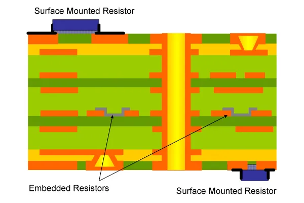
What Are Embedded Components in PCB Design?
Embedded components refer to electronic parts—such as resistors, capacitors, or integrated circuits (ICs)—that are placed within the layers of a PCB rather than mounted on its surface. Unlike traditional surface-mount technology (SMT) or through-hole methods, these components are buried inside the board during the fabrication process. This can involve discrete components placed on an inner layer or passive elements formed directly within the substrate.
The process typically starts with creating cavities or recesses in the PCB layers, where components are then embedded and connected using microvias or copper traces. For example, a resistor might be formed by depositing resistive material between copper layers, achieving values like 50 ohms with a tolerance of ±15%. This integration reduces the need for external solder joints, cutting parasitic inductance—often by as much as 50% compared to SMT—and enhancing electrical performance.
Why Embedded Components Are a Game-Changer
So, what's driving the shift to embedded components? It's all about solving modern engineering challenges. Here are the key benefits that make this technology stand out:
- Space Savings: Embedding components can shrink PCB surface area by up to 35%, as seen in compact wearables like health trackers. This frees up room for more functionality or allows for sleeker designs.
- Improved Signal Integrity: Shorter interconnects reduce parasitic effects. For high-frequency circuits operating at 40–50 GHz, signal loss due to embedded resistors is often negligible—sometimes less than 0.1 dB—compared to SMT alternatives.
- Enhanced Reliability: Without exposed solder joints, embedded components resist shock, vibration, and temperature swings better. This is critical for applications like automotive electronics, where boards might endure 170°C heat cycles.
- Better Thermal Management: Heat dissipates more evenly across the board, reducing hotspots. Thermal vias placed near embedded ICs can lower thermal resistance by 20–30%, improving longevity.
These advantages don't come without trade-offs, though. Embedded designs can increase manufacturing complexity and cost—sometimes by 15–25%—and components can't be easily replaced or tested post-assembly. Still, for high-performance or compact applications, the pros often outweigh the cons.
Suggested Reading: PCB Size Considerations for Embedded Systems: Balancing Space and Functionality
Innovations Driving Embedded Component Technology
The rise of embedded components isn't just a trend—it's fueled by cutting-edge innovations that make them more practical and powerful. Let's look at some of the latest advancements:
Advanced Fabrication Techniques
Laser drilling and multilayer pressing have revolutionized how we embed components. Lasers create precise cavities with depths controlled to within 10 microns, ensuring components fit snugly. For instance, Würth Elektronik's "SOLDER.embedding" process solders SMD parts onto inner layers before pressing them into a multilayer structure, achieving high reliability for automotive applications.
Microvia Technology
Microvias—tiny holes as small as 50 microns—connect embedded components to surface layers. This allows for dense routing and signal paths as short as 0.1 mm, cutting inductance to below 1 nH in some cases. This is a boon for HDI designs, where every millimeter counts.
Formed Passives
Instead of placing discrete parts, some resistors and capacitors are now "formed" within the PCB using resistive or dielectric materials. A formed resistor might achieve 100 ohms with a ±5% base tolerance, adjusted during etching to hit precise values. This reduces assembly steps and boosts consistency.
Wide Bandgap (WBG) Integration
Embedding silicon carbide (SiC) or gallium nitride (GaN) devices into PCBs is gaining traction for power electronics. These WBG semiconductors switch at speeds up to 100 kHz, and embedding them reduces parasitic inductance by 30–40%, as seen in a 10 kW inverter design by Schweizer Electronic.
Real-World Use Cases of Embedded Components
Theory is great, but let's get practical. Here's how embedded components are making a difference in real applications:
Wearable Health Trackers
Imagine a fitness band that monitors heart rate and syncs data wirelessly—all in a slim, lightweight package. Embedding resistors and capacitors beneath the microcontroller cuts the PCB size by 35%, as demonstrated in a prototype by PCBOnline. Shorter signal paths also boost wireless transmission reliability, achieving a stable 2.4 GHz connection with minimal power loss.
Automotive Traction Inverters
Electric vehicles (EVs) rely on efficient power conversion. Infineon's 1200 V CoolSiC™ MOSFETs, embedded using Schweizer's p2PACK® technology, deliver a 50 kW half-bridge design with low thermal impedance. The result? A 35% performance boost over traditional packaging, thanks to reduced switching losses and better heat dissipation.
High-Frequency RF Systems
In RF attenuators tested up to 60 GHz, embedded resistors showed excellent performance with signal loss under 0.2 dB. By placing terminating resistors directly beneath a BGA package, engineers shortened connection lengths to 0.5 mm, slashing parasitic capacitance and improving signal integrity for 5G applications.
Aerospace Sensors
Miniaturized sensors in satellites benefit from embedded passives. A design embedding capacitors within a multilayer PCB reduced weight by 20% and withstood vibrations up to 50 G, meeting stringent UL and IPC standards. This compactness is vital when every gram counts.
Design Considerations for Embedded Components
Ready to incorporate embedded components into your next PCB? Here are some practical tips to keep in mind:
- Placement Precision: Align components with die bonds for direct connections. A misalignment of just 25 microns can increase resistance by 10%, so use CAD tools with tight tolerances.
- Thermal Planning: Add thermal vias near high-power components. For a 1 W resistor, 4–6 vias with 0.3 mm diameter can cut thermal resistance by 25%.
- Tolerance Management: Embedded resistors often have a 15–20% tolerance due to etching variations. Design with consistent impedance—say, 50 ohms across traces—to maintain performance.
- Manufacturability: Consult your fabricator early. Quick-turn prototyping (1–3 days) isn't usually feasible with embedded designs, so plan for longer lead times—typically 5–7 days.
These steps ensure your design leverages the full potential of embedded technology while avoiding common pitfalls.
Recommended Reading: Thermal Management Breakthrough: Using Embedded Components for Efficient PCB Cooling
Challenges and Future Outlook
Despite their promise, embedded components face hurdles. Higher upfront costs—sometimes 20% more than SMT designs—can deter adoption for budget-sensitive projects. Testing is trickier, too; once embedded, a faulty capacitor can't be swapped out without scrapping the board. And while innovations like microvia embedding are advancing, scaling them for mass production remains a work in progress.
Looking ahead, we see embedded technology evolving with 3D integration and IoT demands. By 2030, analysts predict 50% of HDI PCBs will use embedded components, driven by needs for smarter, smaller devices. Advances in materials—like FR4 alternatives with 0.5 W/mK thermal conductivity—could further boost performance and cut costs.
How ALLPCB Supports Embedded Component Designs
For engineers tackling embedded component projects, partnering with the right manufacturer is key. ALLPCB offers advanced manufacturing capabilities tailored to these designs, including quick-turn prototyping in as little as 5 days and precise HDI fabrication with microvias down to 50 microns. Our global logistics ensure fast delivery, while our one-on-one engineering support helps refine your design for manufacturability—whether it's optimizing a 100-ohm embedded resistor or integrating a SiC module. With certifications like ISO 9001:2015 and IPC-A-600 Class 3, we're equipped to bring your innovative PCB to life.
Conclusion
Embedded components in PCB design are more than a trend—they're a revolution in how we approach electronics. By saving space, enhancing performance, and opening new possibilities, they're powering everything from wearables to EVs. Innovations like microvia technology and WBG integration are pushing the boundaries further, while real-world use cases prove their value. For engineers, mastering this technology means balancing benefits with challenges like cost and complexity—but the payoff is worth it. As we move toward a future of smarter, smaller devices, embedded components will be at the heart of the next big breakthrough. Ready to explore this in your designs? We're here to help you make it happen.


