ALLPCB


When designing embedded systems, one of the most critical decisions is determining the right PCB size. For engineers working on compact devices like wearables, IoT gadgets, or automotive control units, PCB size for embedded systems directly impacts functionality, performance, and manufacturability. Striking a balance between space constraints and the need for robust performance is no easy task. In this comprehensive guide, we’ll explore the key factors in embedded system design, focusing on component density, PCB layout, and power consumption to help you optimize your next project.
At its core, the size of a printed circuit board (PCB) in embedded systems must accommodate all necessary components while fitting within the physical limits of the device. Too large, and it won’t fit; too small, and you risk overcrowding, heat buildup, or signal issues. Let’s dive into the specifics of how to approach PCB size considerations and achieve the perfect balance between space and functionality.
Why PCB Size Matters in Embedded System Design
In embedded systems, where devices are often small and portable, PCB size is a defining factor. Whether you’re designing a smartwatch, a medical sensor, or an industrial controller, the PCB must fit within tight spatial constraints while maintaining reliability. A well-optimized PCB size ensures that the system performs efficiently without compromising on critical aspects like signal integrity or thermal management.
Beyond physical fit, PCB size influences manufacturing costs and power efficiency. Larger boards may increase material costs, while overly compact designs can lead to higher assembly complexity due to tight component spacing. Understanding the trade-offs is essential for successful embedded system design.
Key Factors in Determining PCB Size for Embedded Systems
When planning the size of a PCB for embedded systems, several interconnected factors come into play. Below, we break down the most important considerations to guide your design process.
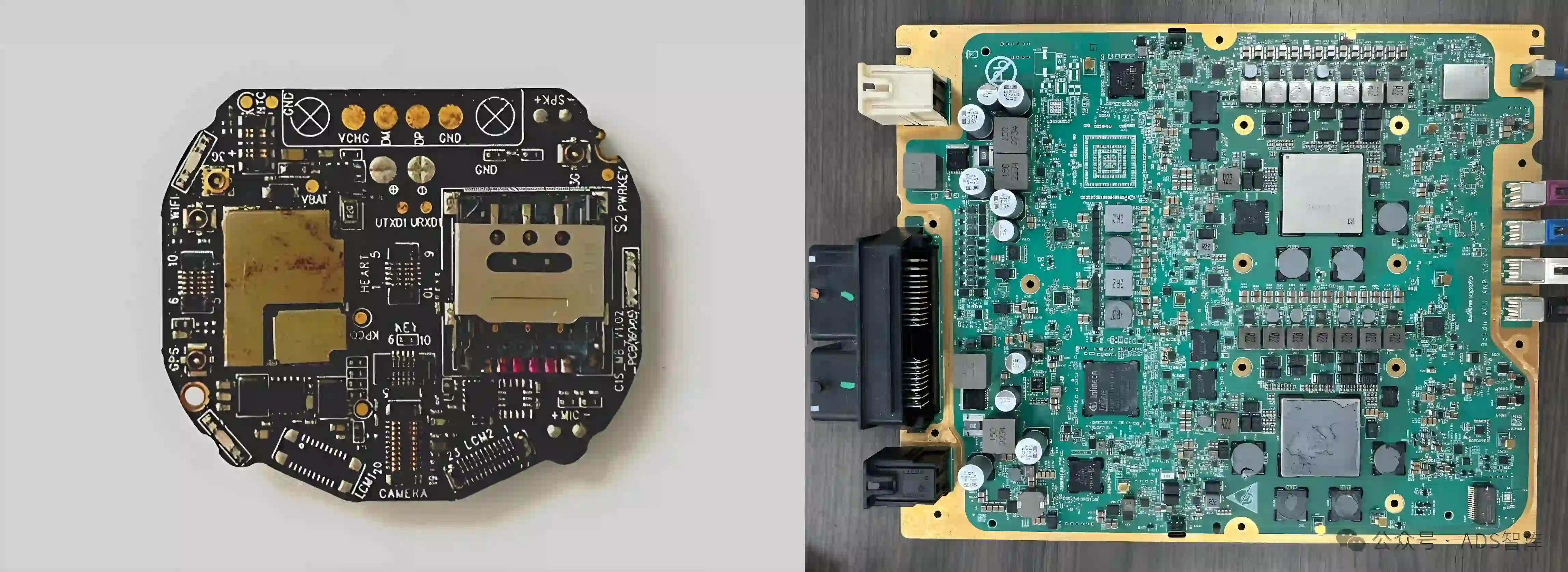
1. Component Density and Placement
Component density refers to how many electronic parts—such as microcontrollers, sensors, resistors, and capacitors—are packed onto a PCB. In embedded systems, where space is limited, achieving high component density is often necessary. However, cramming too many components into a small area can lead to issues like overheating, signal interference, and assembly challenges.
To optimize component density:
- Use surface-mount technology (SMT) components, which are smaller than through-hole parts and allow for tighter layouts.
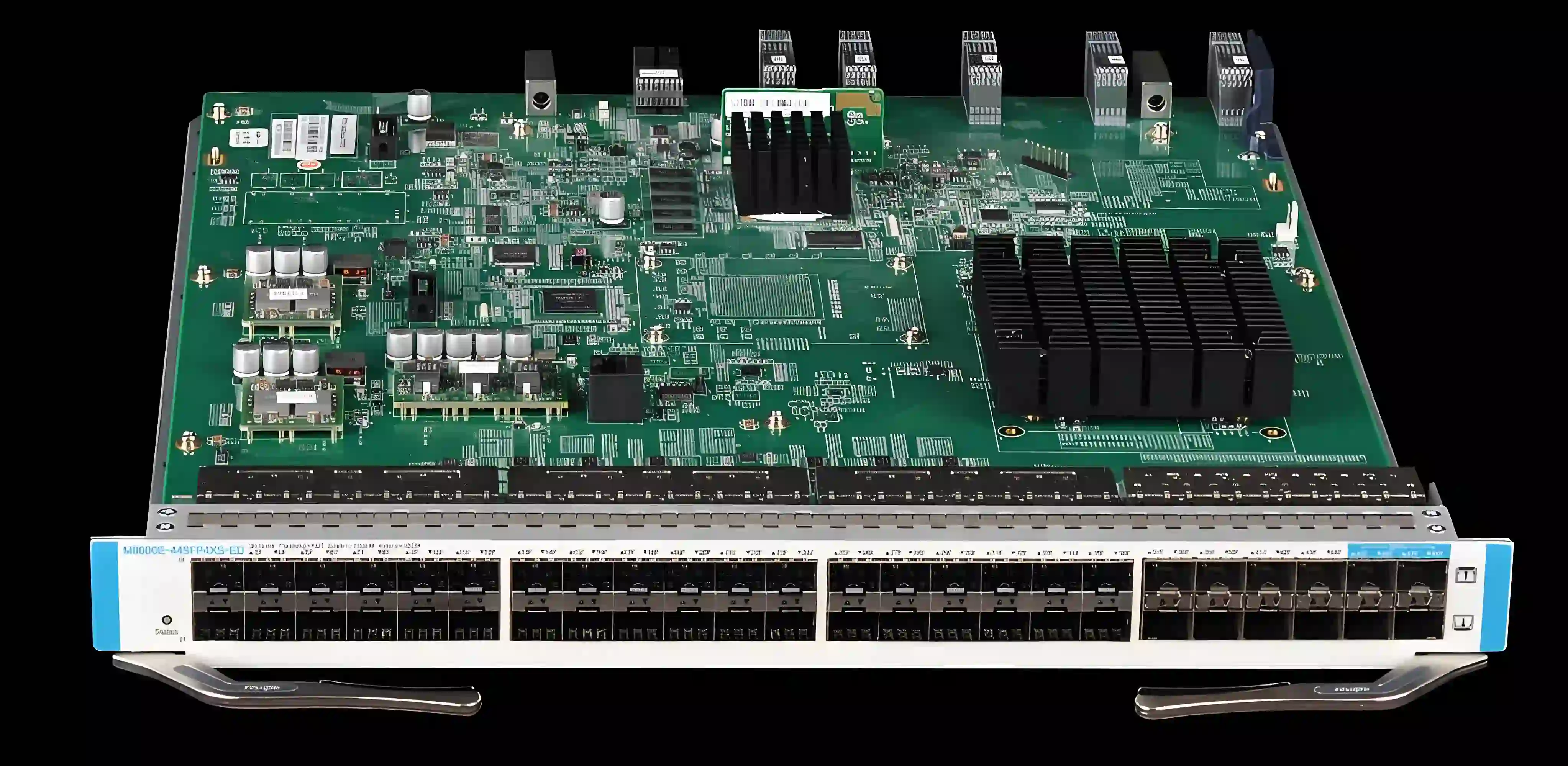
- Prioritize multi-layer PCBs to stack components vertically, reducing the board’s footprint. For example, a 4-layer PCB can house twice as many traces and components as a single-layer board in the same area.
- Group related components together to minimize trace lengths and reduce electromagnetic interference (EMI). For instance, placing a microcontroller close to its supporting capacitors can lower noise levels.
Keep in mind that high component density often requires advanced manufacturing techniques, which can increase costs. A good rule of thumb is to aim for a density that balances functionality with manufacturability—typically, maintaining at least 0.5 mm spacing between components for standard assembly processes.
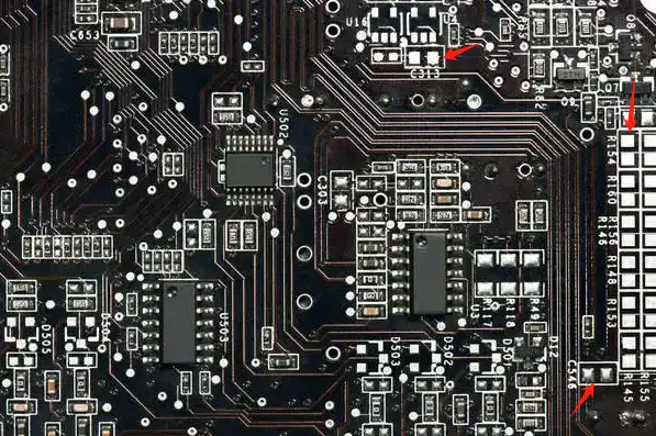
2. PCB Layout and Signal Integrity
The PCB layout is the blueprint that dictates how components are arranged and connected. A poorly planned layout can lead to signal integrity issues, especially in high-speed embedded systems where data rates can exceed 100 MHz. PCB size plays a crucial role here—smaller boards often mean shorter trace lengths, which can reduce signal delays and losses.
However, shrinking the PCB size too much can force traces to be routed too closely, increasing the risk of crosstalk. For example, in a design with a 50-ohm impedance requirement for high-speed signals, maintaining proper trace spacing (often 3 times the trace width) becomes challenging on a tiny board. To mitigate this:
- Use ground planes to shield sensitive signals and reduce noise.
- Route high-speed traces on inner layers of a multi-layer PCB to minimize interference.
- Keep power and ground traces wide to handle current without voltage drops—typically, a trace width of 0.25 mm can carry 1 A safely at 1 oz copper thickness.
A well-thought-out PCB layout ensures that signal integrity is preserved, even when working with limited space in embedded system design.
3. Power Consumption and Thermal Management
Power consumption is a critical concern in embedded systems, especially for battery-powered devices like IoT sensors or wearable tech. The size of the PCB directly affects power efficiency and heat dissipation. Smaller boards have less surface area to dissipate heat, which can lead to thermal buildup if not managed properly.
For instance, a microcontroller running at 3.3V and drawing 100 mA generates heat that must be dissipated. On a compact PCB of 25 mm x 25 mm, this heat can raise the board temperature by 10-15°C above ambient if no thermal relief is provided. To address power consumption and thermal challenges:
- Incorporate thermal vias to transfer heat from hot components to a ground plane or external heat sink.
- Use low-power components whenever possible. For example, choosing a microcontroller with a sleep mode current of under 1 μA can extend battery life significantly.
- Place high-power components, like voltage regulators, near the board’s edges for better airflow or heat sinking.
Balancing power consumption with PCB size ensures that your embedded system remains efficient and reliable over long-term use.
4. Form Factor and Device Constraints
The physical dimensions of the final product often dictate PCB size for embedded systems. For example, a fitness tracker may require a PCB no larger than 20 mm x 30 mm to fit inside a slim wristband. Similarly, automotive embedded systems must conform to specific module sizes defined by industry standards.
When dealing with strict form factor requirements:
- Start by defining the maximum allowable PCB dimensions based on the enclosure or mounting space.
- Consider irregular PCB shapes if a rectangular board doesn’t fit—custom shapes can maximize space usage in tight designs.
- Explore flexible or rigid-flex PCBs for applications where the board must bend or fold to fit, such as in wearable devices.
Aligning the PCB size with the device’s form factor ensures seamless integration without sacrificing functionality.
Strategies to Optimize PCB Size in Embedded Systems
With the challenges of PCB size in mind, let’s explore practical strategies to optimize your design for embedded systems. These approaches focus on maximizing functionality while minimizing space.
1. Adopt Multi-Layer Designs
Multi-layer PCBs are a go-to solution for compact embedded systems. By stacking multiple layers of conductive traces (often 4, 6, or 8 layers), you can fit more circuitry into a smaller footprint. For example, a 4-layer board with dimensions of 30 mm x 40 mm can support the same component count as a single-layer board twice that size.
While multi-layer designs increase manufacturing costs—sometimes by 20-30% per additional layer—they are often worth the investment for high-density applications.
2. Leverage Miniaturized Components
Advancements in component technology have led to smaller, more efficient parts. For instance, 0402 package resistors and capacitors (measuring just 1.0 mm x 0.5 mm) take up far less space than older 0805 packages (2.0 mm x 1.25 mm). Similarly, modern microcontrollers come in compact QFN or BGA packages that save board space while offering powerful performance.
Switching to miniaturized components can reduce PCB size by up to 40%, though it may require finer assembly processes and tighter design rules.
3. Integrate Embedded Components
Embedding passive components like resistors and capacitors directly into the PCB substrate is an emerging technique for ultra-compact designs. This approach eliminates the need for surface-mounted parts, freeing up valuable board space. While still a specialized process, embedding can reduce PCB size by 10-15% in high-density embedded systems.
Common Pitfalls to Avoid in PCB Size Planning
Designing a PCB for embedded systems is fraught with potential missteps. Here are some common pitfalls to watch out for:
- Overcrowding Components: Packing too many parts into a small area can lead to soldering defects and heat issues. Always adhere to minimum spacing guidelines, such as 0.2 mm between SMT pads.
- Ignoring Thermal Needs: Failing to account for heat dissipation on a small PCB can cause component failure. Ensure adequate thermal vias or heat sinks are included.
- Neglecting Signal Integrity: Shrinking PCB size without proper trace routing can degrade performance. Maintain impedance control (e.g., 50 ohms for RF signals) and avoid sharp bends in traces.
Conclusion: Achieving the Perfect Balance
Determining the ideal PCB size for embedded systems is a delicate balancing act. By carefully considering component density, PCB layout, power consumption, and form factor constraints, you can create a design that fits within spatial limits while delivering top-notch performance. Strategies like multi-layer boards, miniaturized components, and embedded technology offer practical ways to optimize space without sacrificing functionality.
Ultimately, successful embedded system design hinges on thorough planning and attention to detail. Take the time to analyze your project’s specific needs, simulate layouts, and test prototypes to ensure that your PCB size supports both current and future requirements. With the right approach, you can build compact, efficient, and reliable embedded systems that stand out in today’s competitive market.