 ALLPCB


In the fast-paced world of electronics manufacturing, ensuring the quality of printed circuit boards (PCBs) is critical. Detecting flaws early in the manufacturing process saves time, reduces costs, and prevents defective products from reaching customers. PCB inspection equipment plays a vital role in achieving this goal, using advanced technologies and methods to spot issues like misaligned components, poor solder joints, and hidden defects. Whether it's through automated systems or manual tools, early detection is the key to high-quality PCB production.
In this blog, we'll dive deep into the importance of PCB inspection equipment and explore various methods such as AOI systems for PCB inspection, X-ray inspection of PCBs, manual PCB inspection microscopes, solder joint inspection, and component placement verification. Let's uncover how these tools and techniques help manufacturers maintain top-notch quality standards.
Why Early Flaw Detection Matters in PCB Manufacturing
The PCB is the backbone of any electronic device, connecting components and ensuring proper functionality. A single flaw, such as a misplaced component or a weak solder joint, can lead to device failure, safety hazards, or costly recalls. Detecting these issues early in the manufacturing process offers several benefits:
- Cost Savings: Fixing a defect during production is far cheaper than addressing it after assembly or in the field. For instance, rework costs can be reduced by up to 80% when flaws are caught before final assembly.
- Improved Yield: Early detection minimizes the number of defective boards, boosting overall production yield rates.
- Enhanced Reliability: Identifying and correcting issues ensures that the final product meets performance and safety standards.
With the complexity of modern PCBs increasing—featuring smaller components and denser layouts—relying on robust inspection equipment is more important than ever. Let's explore the key tools and methods used to achieve this.
Key PCB Inspection Equipment and Techniques
PCB inspection involves a variety of tools and methods, each suited to different stages of the manufacturing process and types of defects. Below, we’ll break down the most common approaches, focusing on their applications and benefits.
1. AOI Systems for PCB Inspection
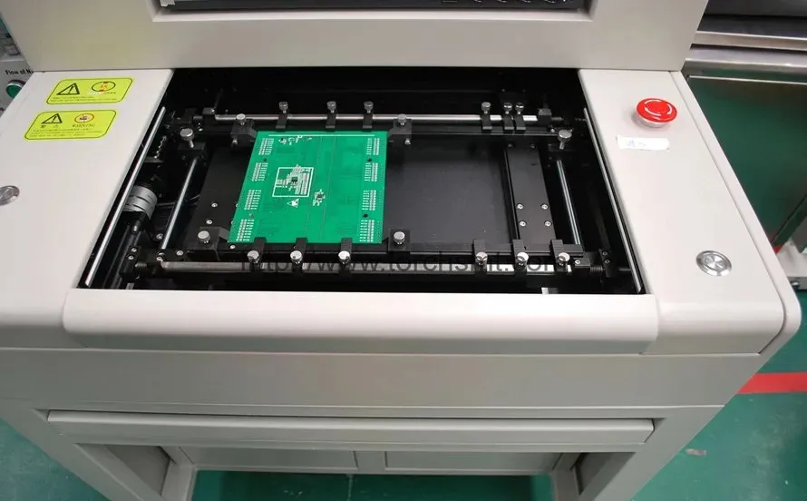
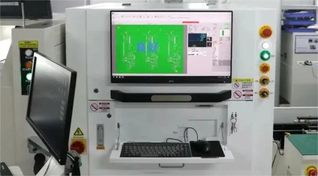
Automated Optical Inspection (AOI) systems are a cornerstone of modern PCB manufacturing. These systems use high-resolution cameras and advanced image processing software to scan PCBs for defects without human intervention. AOI is widely used at multiple stages, including after solder paste application, pre-reflow, and post-reflow soldering.
How AOI Works: The system captures detailed images of the PCB surface and compares them against a pre-defined template or design file. It can detect issues like:
- Missing or misaligned components
- Solder bridges or insufficient solder
- Incorrect component polarity
Benefits of AOI: AOI systems are incredibly fast, often inspecting hundreds of boards per hour, and they provide consistent results compared to manual methods. For example, a typical AOI system can achieve defect detection rates of over 95%, significantly reducing the risk of human error.
Limitations: While highly effective for surface-level defects, AOI cannot detect hidden issues like internal voids in solder joints or defects under components. This is where other methods come into play.
2. X-Ray Inspection of PCBs
For defects that aren't visible on the surface, X-ray inspection of PCBs is an invaluable tool. This method uses X-ray imaging to penetrate the board and reveal internal structures, making it ideal for inspecting hidden solder joints, especially in complex assemblies like Ball Grid Arrays (BGAs).
How X-Ray Inspection Works: The equipment emits low-dose X-rays through the PCB, capturing images of internal layers and connections. Manufacturers can then identify issues such as:
- Voids or cracks in solder joints
- Misaligned pins under surface-mount components
- Internal trace damage
Benefits of X-Ray Inspection: This method is non-destructive and highly accurate, often detecting defects with a precision of up to 99%. It’s particularly useful for high-density boards where traditional visual methods fail. For instance, in a BGA component with hundreds of solder balls, X-ray inspection can reveal voids as small as 0.1 mm in diameter.
Limitations: X-ray systems are more expensive and slower than AOI, making them less suitable for high-volume, rapid inspections. They’re typically used selectively for critical components or during quality audits.
3. Manual PCB Inspection Microscopes
While automation is transforming PCB inspection, manual PCB inspection microscopes remain a vital tool, especially for small-scale production or detailed troubleshooting. These microscopes provide high magnification, allowing technicians to visually inspect boards for defects that automated systems might miss.
How Manual Inspection Works: Technicians use stereo or digital microscopes with magnifications ranging from 10x to 100x to examine specific areas of a PCB. They look for issues like:
- Surface scratches or contamination
- Fine solder joint irregularities
- Component alignment issues
Benefits of Manual Inspection: This method offers flexibility and is cost-effective for low-volume runs. It’s also essential for verifying defects flagged by automated systems. For example, a technician might use a microscope to confirm a solder bridge detected by AOI, ensuring no false positives.
Limitations: Manual inspection is time-consuming and prone to human error, especially over long periods. It’s not practical for large-scale production, where consistency and speed are critical.
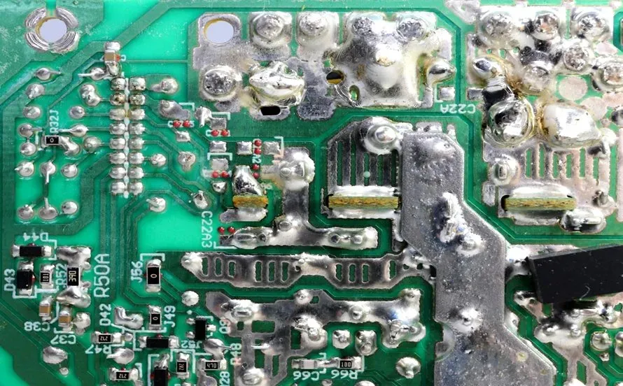
4. Solder Joint Inspection Techniques
Solder joints are the critical connections between components and the PCB, and their quality directly impacts a device’s performance. Solder joint inspection is a specialized focus area that uses multiple methods to ensure reliability.
Common Techniques for Solder Joint Inspection:
- Visual Inspection: Using AOI or manual microscopes to check for surface-level issues like insufficient solder or bridges.
- X-Ray Imaging: Detecting internal defects like voids or cracks, especially in hidden joints under components.
- Thermal Imaging: Identifying poor connections by detecting abnormal heat patterns during operation.
Importance of Solder Joint Quality: A single weak joint can cause intermittent failures or complete device breakdowns. Studies show that over 60% of PCB failures are linked to solder joint issues, making this a priority area for inspection. For high-reliability applications, such as aerospace or medical devices, solder joint inspection often adheres to strict standards like IPC-A-610, which defines acceptable joint shapes and sizes.
5. Component Placement Verification
Ensuring that components are placed correctly on a PCB is a fundamental step in manufacturing. Component placement verification checks for alignment, orientation, and presence of components before and after soldering.
How Verification Works:
- Pre-Reflow AOI: Scans the board after component placement but before soldering to confirm correct positioning.
- Post-Reflow AOI: Verifies that components haven’t shifted during soldering and are still correctly aligned.
- Manual Checks: Used for smaller runs or to double-check automated findings, often with the aid of design files.
Benefits of Verification: Incorrect placement can lead to short circuits, open connections, or device malfunctions. By catching these issues early, manufacturers can avoid costly rework. For instance, a misaligned capacitor with a tolerance of just 0.2 mm can disrupt signal integrity, leading to performance issues at high frequencies (e.g., above 1 GHz).
Choosing the Right Inspection Method for Your Needs
Selecting the appropriate PCB inspection equipment depends on several factors, including production volume, board complexity, and budget. Here’s a quick guide to help manufacturers decide:
- High-Volume Production: Invest in AOI systems for speed and consistency, supplemented by X-ray inspection for critical components.
- Low-Volume or Prototyping: Manual PCB inspection microscopes offer a cost-effective solution for detailed checks.
- Complex Assemblies: Use X-ray inspection for hidden defects and combine with AOI for comprehensive coverage.
- Critical Applications: Prioritize rigorous solder joint inspection and component placement verification to meet strict standards.
By integrating multiple methods, manufacturers can create a robust inspection process that catches flaws at every stage of production.
Future Trends in PCB Inspection Technology
The field of PCB inspection is evolving rapidly, driven by advancements in automation and artificial intelligence (AI). Some emerging trends include:
- AI-Powered AOI: Machine learning algorithms are improving defect detection rates by adapting to new defect patterns, achieving accuracies above 98% in some cases.
- 3D Inspection: Newer AOI and X-ray systems provide three-dimensional imaging for more detailed analysis of complex boards.
- Integration with IoT: Inspection equipment is increasingly connected to factory systems, enabling real-time data sharing and predictive maintenance.
These innovations promise to make PCB inspection faster, more accurate, and more cost-effective, ensuring even higher quality in future electronics.
Conclusion: Building Quality with PCB Inspection Equipment
Detecting flaws early in the PCB manufacturing process is essential for producing reliable, high-performing electronics. From AOI systems for PCB inspection to X-ray inspection of PCBs, manual PCB inspection microscopes, solder joint inspection, and component placement verification, each method offers unique strengths in identifying and addressing defects. By leveraging the right combination of tools and techniques, manufacturers can minimize costs, improve yield, and deliver products that meet the highest quality standards.
At ALLPCB, we’re committed to supporting manufacturers with cutting-edge solutions and expertise in PCB production and inspection. Whether you’re scaling up production or refining a prototype, understanding and implementing effective inspection strategies is the foundation of success in electronics manufacturing.


