 ALLPCB


Introduction
In the evolving landscape of printed circuit board manufacturing, FR-4 remains a cornerstone material due to its balance of cost, reliability, and performance. Advanced techniques like high-density interconnect (HDI) and microvias enable engineers to pack more functionality into smaller footprints using FR-4 substrates. These methods address the demands of modern electronics, where miniaturization drives the need for finer features and denser routing. FR-4 PCB HDI design pushes the limits of this standard laminate through precise processes such as laser drilling and sequential lamination. This article explores these techniques from a manufacturing perspective, offering factory-driven insights for electric engineers optimizing high-density routing FR-4 boards. Understanding these approaches ensures compliance with industry benchmarks while enhancing signal integrity and thermal management.
What Is HDI and Microvias in FR-4 PCBs and Why It Matters
High-density interconnect (HDI) refers to PCB structures that achieve superior wiring density compared to conventional boards, primarily through the use of microvias and finer line widths. Microvia FR-4 implementations involve vias with diameters typically under 150 microns, formed to connect inner layers without penetrating the entire board stack. In FR-4 contexts, HDI allows for integration of fine-pitch components, reducing overall board size and improving electrical performance. This matters for electric engineers facing constraints in consumer devices, automotive systems, and telecommunications equipment, where space and speed are critical. Factory production of microvia FR-4 PCBs demands specialized equipment and process controls to maintain yield and reliability. As devices incorporate more FR-4 PCB fine-pitch components, HDI techniques become essential for achieving high-density routing FR-4 without shifting to exotic materials.
The relevance stems from FR-4's widespread availability and proven track record in multilayer boards. HDI elevates FR-4 from standard applications to advanced PCB manufacturing FR-4 scenarios, supporting blind, buried, and stacked vias. Engineers benefit from shorter signal paths that minimize crosstalk and latency. From a manufacturing viewpoint, these techniques optimize material utilization and streamline assembly. Ultimately, mastering FR-4 PCB HDI design enables cost-effective solutions for high-performance needs.
Technical Principles of HDI and Microvias in FR-4
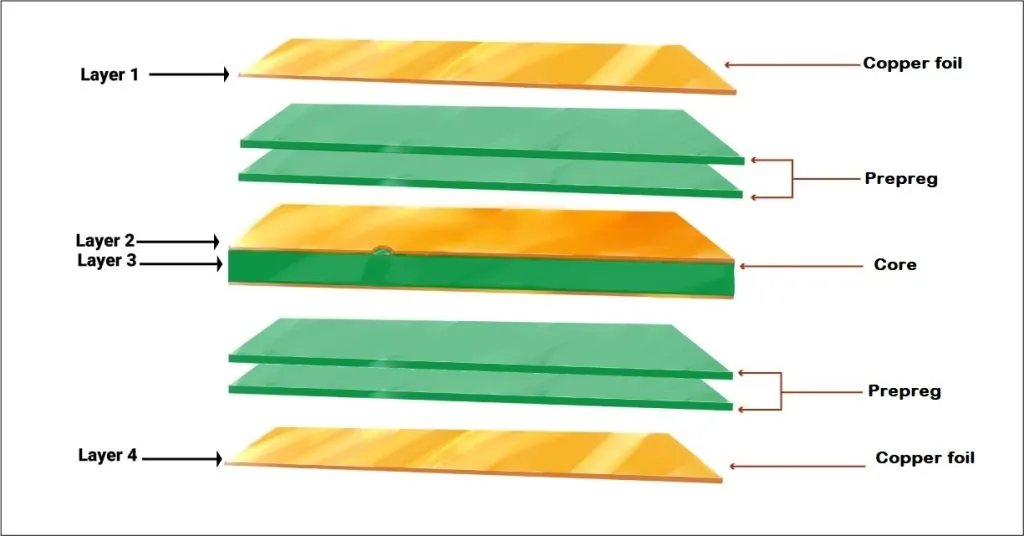
The foundation of HDI in FR-4 lies in microvia formation, where laser drilling FR-4 substrates creates precise openings through copper foil and dielectric layers. UV or CO2 lasers ablate material selectively, producing tapered or straight-walled vias with aspect ratios suitable for electroplating. This process suits FR-4's epoxy-glass composition, as the resin vitrifies cleanly under laser energy, minimizing residue. Post-drilling, desmear operations remove debris, ensuring void-free plating. Sequential lamination FR-4 builds upon this by incrementally adding layers, lamination cycles align and bond sub-stacks with microvias already formed in outer layers.
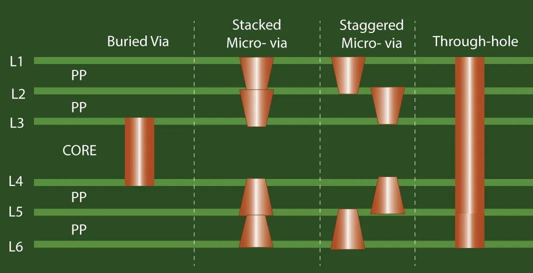
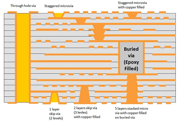
HDI structures classify into types based on via configurations: passive (single microvia layer), active (microvias on both sides of core), and pressed or ELIC (every layer interconnect). In FR-4, sequential lamination involves multiple build-up steps, where intermediate laminations encapsulate vias before drilling new ones. This method controls registration accuracy, critical for high-density routing FR-4. Copper filling or plating techniques then metallize vias, providing planar surfaces for subsequent routing. Factory processes emphasize uniform resin flow during lamination to prevent voids that could compromise integrity.
Aspect ratios for microvias in FR-4 typically stay below 1:1 to facilitate plating chemistry penetration. Staggered via placement distributes stress and enhances thermal dissipation. These principles align with established guidelines like IPC-2226, which outlines design considerations for HDI features. Manufacturing sequences prioritize layer-to-layer alignment, often using fiducials for optical registration. The result is a robust FR-4 structure capable of supporting advanced PCB manufacturing FR-4 demands.
Related Reading: Mastering Microvia Formation in HDI Assembly: Laser Drilling Techniques
Best Practices for FR-4 PCB HDI Design and Manufacturing
Effective FR-4 PCB HDI design starts with stack-up planning, balancing core thickness, prepreg count, and via fanout for FR-4 PCB fine-pitch components. Engineers should prioritize via-in-pad configurations for BGAs with pitches under 0.5 mm, ensuring escape routing fits within microvia capabilities. High-density routing FR-4 requires line widths and spaces down to 50 microns, necessitating controlled impedance modeling early. Sequential lamination FR-4 benefits from symmetric builds to minimize warpage, with outer layers using thinner dielectrics for tighter vias.
In production, laser drilling FR-4 demands optimized parameters like pulse energy and scan speed to achieve clean sidewalls. Post-laser plasma cleaning enhances adhesion for plating. Factories implement sequential build-ups with intermediate inspections to verify via continuity and resist cracking. For microvia FR-4 reliability, avoid excessive stacking; limit to two levels unless qualified otherwise. Copper-filled vias provide better planarization for fine-line imaging.
Related Reading: HDI PCB Manufacturing Process: A Step-by-Step Guide for Engineers
Adherence to IPC-6016 qualification specs ensures HDI boards meet performance criteria under thermal cycling and shock. Best practices include fanout optimization, where microvias directly under pads reduce inductance. Thermal management integrates filled vias near power planes. Yield improves with design rules like minimum land sizes and anti-pad clearances. These steps make advanced PCB manufacturing FR-4 viable for production volumes.
Challenges in Microvia FR-4 HDI and Factory Solutions
One key challenge in microvia FR-4 is via reliability under thermal stress, as CTE mismatch between copper and FR-4 can induce cracks. Sequential lamination FR-4 exacerbates this if lamination pressures vary, leading to resin-rich zones. Factories counter with high-Tg FR-4 grades that withstand multiple reflows. Laser drilling FR-4 risks carbon residue if parameters drift, addressed via automated process control and inline AOI.
Registration in high-density routing FR-4 poses issues during multi-step builds, where cumulative tolerances accumulate. Solutions involve precision alignment systems and fiducial arrays on sub-laminates. Plating uniformity in small vias requires pulse-reverse electroplating to avoid dimples. For FR-4 PCB fine-pitch components, solder mask registration must match microvia tolerances.
IPC-6012 provides benchmarks for rigid board acceptability, guiding inspections for voids and barrel quality. Warpage control uses matched CTE foils and constrained lamination. These factory-driven mitigations ensure robust HDI performance.
Conclusion
Advanced FR-4 PCB techniques like HDI and microvias unlock denser, more efficient boards without abandoning proven materials. Laser drilling FR-4, sequential lamination FR-4, and optimized high-density routing FR-4 form the core of these methods, enabling support for FR-4 PCB fine-pitch components. Electric engineers gain from shorter paths, better SI, and compact designs. Factory insights emphasize process control, standard alignment, and iterative qualification. By applying these practices, teams achieve reliable advanced PCB manufacturing FR-4 outcomes. Future iterations will refine these for even higher densities.
FAQs
Q1: What are the main benefits of microvia FR-4 in HDI designs?
A1: Microvia FR-4 enables higher component density and reduced signal path lengths in HDI PCBs, improving speed and minimizing EMI. From a manufacturing standpoint, it supports sequential lamination FR-4 for blind and buried connections without full through-vias. This suits FR-4 PCB fine-pitch components by allowing direct fanout. Reliability holds under standard thermal profiles when aspect ratios are controlled.
Q2: How does laser drilling FR-4 impact HDI production yields?
A2: Laser drilling FR-4 provides precision for microvias under 150 microns, boosting high-density routing FR-4 capabilities. Factories achieve high yields with optimized ablation to avoid residue, followed by desmear. It outperforms mechanical methods for small diameters. Process monitoring ensures consistent sidewall quality per IPC guidelines.
Q3: What role does sequential lamination play in FR-4 PCB HDI design?
A3: Sequential lamination FR-4 builds HDI stacks incrementally, forming microvias layer by layer for complex interconnects. This technique aligns with advanced PCB manufacturing FR-4 needs, enabling active and ELIC structures. It controls thickness and registration for FR-4 PCB HDI design. Proper bonding prevents delamination in multilayer builds.
Q4: Can standard FR-4 handle fine-pitch components in HDI?
A4: Yes, enhanced FR-4 with HDI microvias supports fine-pitch components via via-in-pad and tight routing. High-density routing FR-4 requires careful stack-up to manage impedance. Manufacturing focuses on planarization for assembly. It balances cost and performance for many applications.


