 ALLPCB


Introduction
Panelization plays a crucial role in optimizing double-sided PCB manufacturing processes. By combining multiple individual circuit boards into a single larger panel, manufacturers achieve higher throughput and reduced handling time during fabrication and assembly. This approach is particularly beneficial for double-sided PCBs, where components populate both sides, demanding precise alignment and minimal stress introduction. Efficient panelization techniques enhance PCB production efficiency while maintaining quality standards essential for electrical engineers. As production volumes increase, selecting the right panelization method becomes key to balancing cost, yield, and reliability. Factory-driven insights reveal that thoughtful panel design directly impacts downstream PCB assembly success.
What Is Double-Sided PCB Panelization and Why It Matters
Double-sided PCB panelization involves arranging several identical or mixed circuit boards on a shared substrate for simultaneous processing. This method streamlines PCB manufacturing by allowing automated equipment to handle larger arrays, cutting setup times and material waste. In double-sided configurations, panelization ensures consistent registration between top and bottom layers, critical for via alignment and solder joint integrity. It matters because unoptimized panels lead to inefficiencies like increased scrap rates or assembly defects. For electrical engineers focused on PCB design, understanding panelization supports scalable production without compromising electrical performance. Ultimately, it aligns factory capabilities with design intent for reliable double-sided PCB assembly.
Panelization reduces per-board costs through economies of scale in etching, plating, and soldering steps. Double-sided boards benefit from uniform thermal exposure across the panel, minimizing variations in copper deposition. Engineers must consider panel layout early in PCB design to avoid rework. Factory experience shows that well-panelized arrays improve pick-and-place accuracy during PCB assembly. This technique also facilitates quality control inspections on a larger scale. Relevance grows with rising demands for compact electronics requiring double-sided solutions.
Key Panelization Techniques for Double-Sided PCBs
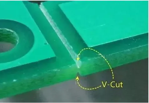
Several established techniques suit double-sided PCB panelization, each with factory-specific advantages. V-scoring creates angled grooves along straight edges, enabling clean separation with specialized tools. This method excels for rectangular boards in high-volume PCB production, as it preserves panel integrity during handling. For double-sided PCBs, V-scoring minimizes exposure of inner layers to stress, supporting multilayer alignment. Factories prefer it for its compatibility with automated depanelization lines. However, it limits irregular shapes, requiring straight-line segmentation.
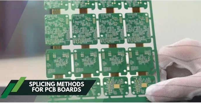
Tab routing uses perforated tabs or bridges to connect boards within the panel. These tabs, often with mouse bites for easier breakup, allow flexible layouts for non-rectangular designs. In double-sided PCB manufacturing, tab routing distributes mechanical loads evenly, reducing risk of delamination during separation. Engineers appreciate its versatility in mixed-array panels, optimizing material use. Factory processes involve routing around board perimeters while leaving robust tabs for stability. This technique proves ideal when V-scoring constraints apply.
A hybrid approach combines V-scoring on outer edges with tab routing for inner separations. This balances efficiency and flexibility, common in complex double-sided PCB assembly workflows. Panels maintain structural rigidity through production, easing fiducial recognition by pick-and-place machines. Electrical engineers benefit from reduced warpage potential in varied board sizes. Factories report higher yields with hybrids for production runs blending board types. Selection depends on board geometry and volume requirements.
Break routing fully mills slots between boards, supported by frame rails. It offers maximum design freedom but demands precise tooling to prevent panel distortion. For double-sided PCBs, this method suits prototypes or low-volume where custom shapes dominate. Factories add tooling holes and fiducials to ensure repeatable handling. While more labor-intensive for depanelization, it avoids groove-related stress concentrations. Engineers use it when other techniques compromise trace routing near edges.
Related Reading: V-Cut vs Tab-Routing: Pros and Cons of PCB Panelization Methods
Best Practices for Double-Sided PCB Panelization in Design and Production
Start with symmetrical panel layouts to counterbalance copper distribution on both sides. Uneven arrays exacerbate thermal stresses during reflow, common in double-sided PCB manufacturing. Incorporate adequate perimeter rails for fixture clamping, preventing edge damage. Fiducial marks at panel corners aid optical alignment in PCB assembly. Factory standards emphasize multiple tooling holes symmetrically placed for vacuum fixturing. These practices align with IPC-2221 design guidelines, ensuring manufacturability from the outset.
Optimize board spacing to allow routing tool clearance without encroaching on components. Keep sensitive traces and vias inset from panel edges to withstand depanelization forces. For double-sided boards, balance component density across sides to minimize bow. Simulate panel stress in PCB design software early. Factories validate layouts via DFM reviews before production. Consistent rail thickness supports stable processing through lamination and plating.
Address warpage proactively by selecting materials with matched coefficients of thermal expansion. Larger panels amplify bow in double-sided configurations due to sequential soldering. Use breakaway tabs with perforations to distribute shear loads evenly. Post-bake panels if needed to relieve internal stresses before assembly. IPC-6012 qualification specs guide acceptance criteria for flatness in rigid boards. Electrical engineers integrate these into PCB production planning for reliable outcomes.
Incorporate process edges on longer board sides for automated handling. These rails host fiducials and tooling holes, streamlining double-sided PCB assembly flows. Avoid placing high-density components near separation lines. Factories recommend rounded corners on rails to reduce stress risers. Validate panel designs through test arrays in initial runs. This factory-driven approach enhances overall PCB manufacturing efficiency.
Challenges in Double-Sided PCB Panelization and Mitigation Strategies
Double-sided panels face heightened warpage risks from asymmetric heating during reflow soldering. Top-side components reflow first, inducing bow that misaligns bottom placements. Larger arrays compound this via cumulative thermal gradients. Mechanical stresses during depanelization can crack vias or lift pads. Factories mitigate via controlled cooling ramps and pallet fixturing. Engineers design copper balancing to neutralize these effects.
Stress concentrations at tabs or scores threaten trace integrity in double-sided boards. V-scoring suits thin substrates but risks splintering thicker ones. Tab routing introduces breakout variability if perforations misalign. IPC-A-600 acceptability criteria evaluate edge quality post-separation. Simulate depanelization forces in PCB design phases. Factory insights stress uniform tab sizing for predictable yields.
Handling larger panels increases contamination exposure between processes. Dust on one board affects the array during double-sided plating. Use covered carriers and cleanroom protocols. Alignment drifts occur if tooling holes lack precision. Redundant fiducials compensate effectively. These strategies sustain quality through PCB production cycles.
Component interference during sequential assembly poses risks in panelized double-sided PCBs. Tall parts on one side snag during flips. Stagger heights and profile components accordingly. Factories sequence reflow passes with gravity-assisted settling. Monitor panel bow inline for early intervention. Robust panelization overcomes these for efficient throughput.
Related Reading: Troubleshooting PCB Panelization Issues: Common Problems and Solutions
Conclusion
Effective panelization techniques transform double-sided PCB manufacturing into a streamlined operation. V-scoring, tab routing, and hybrids each offer tailored benefits for efficiency and reliability. Best practices in layout, fiducials, and stress management prevent common pitfalls like warpage. Electrical engineers gain from factory-aligned designs per industry standards. PCB assembly and production see direct yield improvements. Prioritizing these methods ensures scalable, high-quality double-sided PCB panelization.
FAQs
Q1: What are the main advantages of double-sided PCB panelization in manufacturing?
A1: Double-sided PCB panelization boosts efficiency by processing multiple boards simultaneously, reducing setup times and material costs. It ensures uniform quality across arrays during etching and plating. Factories achieve higher throughput for PCB assembly, with better pick-and-place accuracy via shared fiducials. Alignment consistency minimizes defects in via filling for double-sided layers. This approach suits volume production while maintaining design integrity.
Q2: How does V-scoring compare to tab routing for double-sided PCB production?
A2: V-scoring provides straight-line separations ideal for rectangular double-sided PCBs, lowering depanelization costs. Tab routing offers flexibility for irregular shapes, distributing stresses evenly across both sides. Factories select V-scoring for high-volume runs and tabs for prototypes. Both support PCB manufacturing standards but differ in tool requirements. Choose based on board geometry and assembly needs.
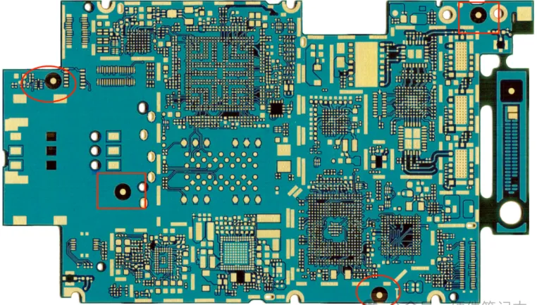
Q3: What role do fiducials play in double-sided PCB panelization?
A3: Fiducials enable precise optical registration for panelized double-sided PCB assembly. Placed at corners and locally near boards, they compensate for minor distortions. In PCB production, they align masks and stencils accurately across arrays. Factories require at least three per panel for robust machine vision. This ensures component placement integrity on both sides.
Q4: How can warpage be minimized in double-sided PCB panelization?
A4: Symmetrical layouts and balanced copper distribution counter thermal stresses in double-sided panels. Adequate rail support and perforations reduce mechanical loads during separation. Factories use controlled reflow profiles and post-bake steps. PCB design incorporates IPC guidelines for flatness. These measures enhance reliability in manufacturing and assembly.
References
IPC-2221B — Generic Standard on Printed Board Design. IPC, 2012
IPC-6012E — Qualification and Performance Specification for Rigid Printed Boards. IPC, 2017
IPC-A-600K — Acceptability of Printed Boards. IPC, 2020


