ALLPCB


If you're an engineer looking to understand the HDI PCB fabrication process, you've come to the right place. High-Density Interconnect (HDI) PCBs are essential for modern electronics, enabling smaller, faster, and more efficient devices. In this comprehensive guide, we'll walk you through the HDI PCB manufacturing process step by step, covering key techniques like sequential lamination HDI PCB and other critical aspects of production. Whether you're designing compact consumer gadgets or complex industrial systems, this blog will equip you with the knowledge to navigate HDI PCB production with confidence.
What Are HDI PCBs and Why Do They Matter?
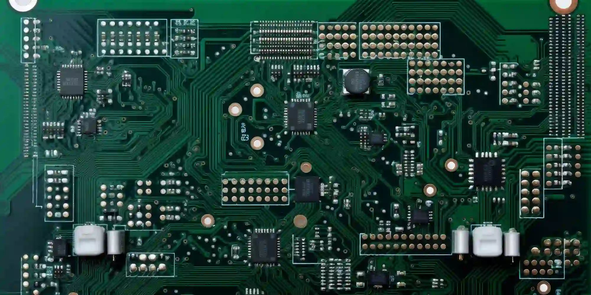
HDI PCBs are a type of printed circuit board designed to pack more components into a smaller space. Unlike traditional PCBs, HDI boards feature finer lines, smaller vias, and higher connection densities. This makes them ideal for smartphones, wearables, medical devices, and automotive systems where space and performance are critical.
The importance of HDI PCBs lies in their ability to support high-speed signals and reduce signal loss. For instance, HDI boards can handle signal speeds up to 5 Gbps or higher in advanced applications, thanks to their reduced layer thickness and optimized impedance control (often targeting 50 ohms for high-frequency signals). Understanding the HDI PCB manufacturing techniques is crucial for engineers to ensure designs meet performance and reliability standards.
Overview of the HDI PCB Manufacturing Process
The HDI PCB fabrication process involves multiple steps, each requiring precision to achieve the desired density and performance. Unlike standard PCB production, HDI manufacturing often includes advanced techniques like sequential lamination and microvia formation. Below, we break down the process into clear, actionable steps to guide engineers through the journey from design to finished board.
Step 1: Design and Planning for HDI PCBs
The process begins with careful design and planning. Engineers must define the board's layer stack-up, via types (blind, buried, or through-hole), and trace widths. HDI designs often use trace widths as small as 3 mils (0.003 inches) and spacing of 3 mils to maximize density. During this phase, impedance requirements and signal integrity are calculated to avoid issues like crosstalk or signal delay.
Software tools are used to simulate the design and identify potential challenges before production. This step is critical because errors in design can lead to costly rework during manufacturing. Engineers should also consider the materials, such as high-frequency laminates or low-loss dielectrics, to meet performance needs.
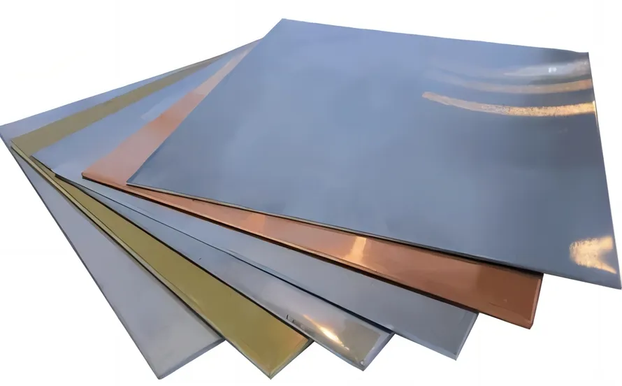
Step 2: Material Selection and Preparation
Choosing the right materials is a cornerstone of the HDI PCB manufacturing process. HDI boards often use thin dielectric layers (as low as 2 mils thick) to reduce overall board thickness. Common materials include FR-4 for cost-effective designs or advanced materials like polyimide for high-temperature or flexible applications.
Once materials are selected, they are cut and prepared for lamination. Copper foil, typically 0.5 to 1 ounce per square foot, is applied to the substrate to form conductive layers. Surface cleanliness is vital at this stage to prevent defects during later steps like etching or drilling.
Step 3: Inner Layer Processing and Imaging
With materials ready, the inner layers of the HDI PCB are processed. A photoresist layer is applied to the copper surface, and the desired circuit pattern is transferred using UV light exposure through a photomask. After developing the photoresist, unwanted copper is etched away, leaving behind the circuit traces.
For HDI PCBs, this step demands high precision due to the fine line widths and tight tolerances. Any misalignment or defect in imaging can compromise the board's functionality, especially for high-speed applications where signal integrity is paramount.
Step 4: Sequential Lamination in HDI PCB Manufacturing
One of the defining techniques in sequential lamination HDI PCB production is building the board layer by layer. Unlike standard PCBs, where all layers are laminated at once, HDI boards use sequential lamination to create complex structures with blind and buried vias.
In this process, individual layer pairs are fabricated, imaged, and etched before being laminated together. After each lamination cycle, vias are drilled and filled to connect the layers. This method allows for higher layer counts (often 6 to 20 layers or more) and greater design flexibility. However, it also increases manufacturing time and cost due to the multiple lamination cycles, sometimes requiring 3 to 5 cycles for a single board.
Sequential lamination ensures reliable interconnects, which are essential for maintaining signal integrity at high frequencies. For example, controlled impedance traces on an HDI board might maintain a tolerance of ±10% to ensure consistent performance.
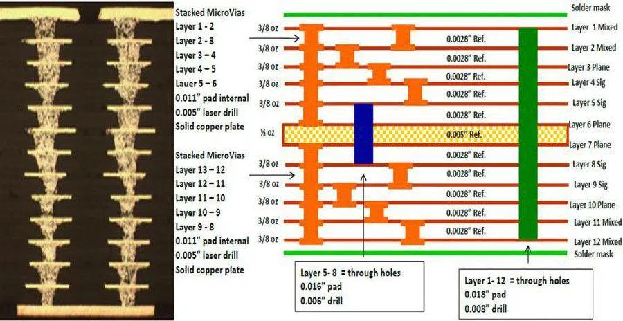
Step 5: Microvia Drilling and Formation
HDI PCBs rely heavily on microvias—tiny holes with diameters as small as 4 mils (0.004 inches)—to connect layers. These vias are typically drilled using laser technology, which offers greater precision than mechanical drilling. Laser drilling can achieve aspect ratios of 0.75:1 or better, ensuring reliable connections even in thin dielectric layers.
Microvias can be blind (connecting an outer layer to an inner layer) or buried (connecting inner layers only). After drilling, the vias are cleaned to remove debris and then plated with copper to establish electrical conductivity. This step is critical in the HDI PCB fabrication process because poorly formed vias can lead to open circuits or signal degradation.
Step 6: Copper Plating and Via Filling
Once microvias are drilled, they are plated with copper to create conductive pathways. Electroplating is commonly used, depositing a uniform copper layer inside the vias and on the board surface. For some HDI designs, vias are filled with conductive or non-conductive paste to prevent voids and enhance structural integrity.
The plating thickness is carefully controlled, often ranging from 0.8 to 1.2 mils, to balance conductivity and manufacturability. Overplating can cause uneven surfaces, while underplating may result in weak connections. This step directly impacts the board's reliability, especially in high-density designs where hundreds of vias are present.
Step 7: Outer Layer Processing and Solder Mask Application
After the inner layers and vias are complete, the outer layers are processed similarly to the inner layers with imaging and etching. A solder mask is then applied to protect the copper traces and prevent short circuits during component assembly. The solder mask also defines the areas where components will be soldered, ensuring precise placement.
For HDI PCBs, the solder mask must be thin and uniform to accommodate fine-pitch components, often with pad sizes as small as 8 mils. Surface finishes like ENIG (Electroless Nickel Immersion Gold) are applied to enhance solderability and protect against oxidation.
Step 8: Electrical Testing and Quality Control
Before the HDI PCB is ready for use, it undergoes rigorous electrical testing to verify continuity, insulation resistance, and impedance. Automated test equipment checks for open circuits, shorts, and other defects. For high-speed designs, time-domain reflectometry (TDR) may be used to measure impedance, ensuring it falls within the specified range (e.g., 50 ± 5 ohms).
Quality control also includes visual inspection and X-ray analysis to detect hidden defects like misaligned vias or incomplete plating. Only boards that pass these stringent checks move to the final stages of production.
Step 9: Final Fabrication and Routing
In the final step, the HDI PCB panel is routed into individual boards using CNC machines or laser cutting. Edges are smoothed to prevent damage during handling, and any additional features like slots or cutouts are added. The boards are then cleaned to remove residues and packaged for shipment.
This step requires precision to avoid damaging the fine traces and vias on HDI boards. Even minor errors can render a board unusable, especially in applications requiring tight tolerances.
Key HDI PCB Manufacturing Techniques to Know
Beyond the basic steps, several advanced HDI PCB manufacturing techniques are worth understanding. These methods allow for even greater density and performance, addressing the needs of cutting-edge technology.
Via-in-Pad Technology
Via-in-pad technology places vias directly under component pads, saving space and improving signal routing. This technique is common in HDI designs for fine-pitch components like BGAs (Ball Grid Arrays) with pitch sizes as small as 0.4 mm. However, it requires precise via filling to ensure a flat surface for soldering.
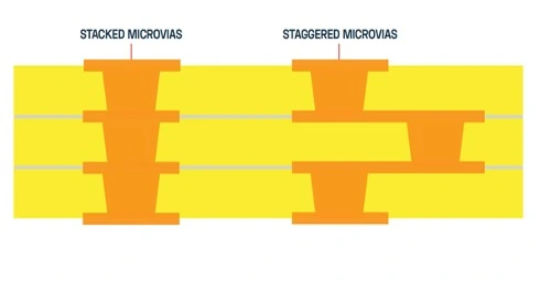
Stacked and Staggered Microvias
Stacked microvias are placed directly on top of each other to connect multiple layers, while staggered microvias are offset to reduce stress on the board. Both approaches are used in HDI PCBs with high layer counts (10 or more) to optimize space and maintain reliability.
Advanced Materials for High Performance
For applications requiring low signal loss, HDI PCBs may use materials with a dielectric constant (Dk) as low as 3.0 and a dissipation factor (Df) of 0.002 or less. These materials minimize signal distortion at frequencies above 1 GHz, making them ideal for 5G and IoT devices.
Challenges in HDI PCB Manufacturing
While HDI PCBs offer numerous benefits, their production comes with challenges. The complexity of sequential lamination and microvia formation increases manufacturing costs, often by 30-50% compared to standard PCBs. Additionally, the tight tolerances and fine features demand advanced equipment and skilled operators, which can lead to longer lead times.
Thermal management is another concern, as the high component density generates more heat in a smaller area. Engineers must design with proper heat dissipation in mind, sometimes incorporating thermal vias or metal cores to manage temperatures effectively.
Benefits of Mastering HDI PCB Fabrication
Despite the challenges, the advantages of HDI PCBs make the effort worthwhile. These boards enable miniaturization, allowing devices to shrink without sacrificing functionality. They also improve electrical performance by reducing signal path lengths, which can lower latency by up to 20% in high-speed designs.
For engineers, understanding the HDI PCB fabrication process provides a competitive edge. It allows for better collaboration with manufacturers, optimized designs, and faster time-to-market for innovative products.
Conclusion: Navigating the Future with HDI PCBs
The HDI PCB manufacturing process is a complex but rewarding journey for engineers. From design and material selection to sequential lamination HDI PCB techniques and final testing, each step plays a vital role in creating high-performance boards. By mastering these HDI PCB manufacturing techniques, you can unlock new possibilities for compact, efficient, and reliable electronics.
Whether you're working on consumer gadgets or industrial systems, the knowledge of HDI PCB production empowers you to push the boundaries of what's possible. With precision and attention to detail, you can ensure your designs meet the demands of today's fast-paced, technology-driven world.