 ALLPCB


Introduction
High-frequency PCB manufacturing involves producing printed circuit boards capable of handling signals above 1 GHz, critical for applications like telecommunications, radar systems, and high-speed data processing. These boards demand precise control over electrical properties to minimize signal loss and maintain integrity. In PCB manufacturing, factors such as material properties, fabrication tolerances, and process consistency play pivotal roles. Engineers must navigate challenges like dielectric losses and impedance variations to ensure reliable performance. This article explores key considerations and best practices in high-frequency PCB fabrication, drawing from factory-driven insights to guide production decisions.
Understanding High-Frequency PCBs and Their Importance
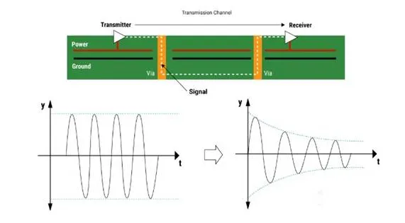
High-frequency PCBs operate at frequencies where wavelength approaches the size of board features, making traditional low-frequency designs inadequate. Signal propagation in these boards is influenced by dielectric constant (Dk), dissipation factor (Df), and conductor surface roughness, which affect attenuation and phase shift. In modern electronics, demand surges from 5G infrastructure, automotive radar, and satellite communications, where even minor manufacturing deviations can degrade performance. PCB fabrication for high frequencies requires tighter tolerances, often below 10% for critical dimensions, compared to standard boards. Why does this matter? Poorly manufactured high-frequency PCBs lead to increased insertion loss, crosstalk, and electromagnetic interference, compromising system reliability.
Factory experience shows that high-frequency boards benefit from specialized laminates with low Df values under 0.005 at 10 GHz to preserve signal quality. Engineers should prioritize designs that account for manufacturing variability, such as copper foil type and resin content uniformity. Adhering to standards like IPC-6018 ensures qualification for microwave applications by specifying performance metrics for high-frequency rigid boards.
Material Selection and Handling in High-Frequency PCB Manufacturing
Material selection forms the foundation of high-frequency PCB manufacturing, focusing on laminates with stable Dk and low Df across temperature and frequency ranges. Reinforced PTFE or ceramic-filled composites offer superior performance but pose handling challenges due to moisture sensitivity and mechanical fragility. Proper material handling prevents absorption, which can alter electrical properties during fabrication. Storage in dry nitrogen cabinets and acclimation before lamination are standard protocols to maintain consistency.
In the factory, material handling extends to ESD protection and cleanroom protocols, as contaminants on surfaces can introduce losses during etching or plating. Panels must undergo plasma cleaning to remove residues without damaging the dielectric. Sequential lamination techniques allow embedding low-loss cores between high-stability prepregs, optimizing stackup for controlled impedance. Engineers verify material certificates for batch uniformity, ensuring Df stability per application requirements.
Related Reading: Choosing the Right Materials for High Frequency PCBs: A Dk and Df Deep Dive

Key Fabrication Processes: Etching and Plating
Etching in high-frequency PCB fabrication demands precision to achieve fine line widths and spaces, often 50 microns or less, to support high-density interconnects. Panel plating followed by tented etchback or direct imaging resists ensures uniform copper removal, minimizing undercuts that cause impedance drift. Factory best practices include using low-etch factor chemistries and endpoint detection to control sidewall profiles, critical for signal integrity.
Plating processes, such as electroless copper deposition and electroplating, fill vias and define traces with smooth surfaces to reduce skin effect losses at high frequencies. For high-frequency boards, reverse pulse plating reduces roughness, improving conductor performance. Post-plating flash etching removes excess copper while preserving line geometry. These steps align with IPC-6012 requirements for rigid board performance, emphasizing dimensional stability and conductor integrity.
Material handling during these stages prevents oxidation or contamination, with automated conveyance systems minimizing human touch. Quality checks via automated optical inspection after etching detect anomalies early, preventing yield losses.
Quality Control in High-Frequency PCB Manufacturing
Quality control permeates every phase of high-frequency PCB fabrication, from incoming inspection to final electrical testing. Cross-section microscopy verifies via plating thickness and drill quality, while time-domain reflectometry (TDR) measures impedance across traces. Factories implement statistical process control to track variations in etching depth and plating uniformity, ensuring compliance with class 3 or higher standards.
Automated X-ray and thermal stress screening detect voids or delamination risks inherent in high-frequency materials. Solderability preservation through immersion tin or ENIG finishes supports assembly without degrading RF performance. Final flying probe or bed-of-nails testing confirms continuity and shorts under operational frequencies.
Adherence to IPC-A-600 criteria for acceptability guides visual and dimensional inspections, flagging issues like mouse bites or measling that could amplify losses.
Best Practices for High-Frequency PCB Manufacturing
Implement design-for-manufacturability (DFM) reviews early, specifying stackup with symmetric builds to avoid warpage. Use blind and buried vias judiciously, optimizing via stub lengths through back-drilling for minimal reflections. In fabrication, maintain tight process windows: drill aspect ratios below 10:1, lamination pressure calibrated for resin flow without voids.
Material handling best practices include baking panels at 125°C for 4 hours pre-drill to desorb moisture, followed by immediate processing. For etching, employ laser direct imaging for photolithography accuracy, coupled with ozone rinse for residue-free surfaces. Plating baths require precise chemistry control, with current density profiling for uniform deposition.
Quality control loops back with 100% AOI and sampling for vector network analyzer (VNA) sweeps up to 40 GHz. Document all process parameters per ISO 9001 quality management systems to enable traceability and continuous improvement. These practices yield boards with insertion loss below 1 dB/inch at 10 GHz, meeting demanding RF applications.
Related Reading: Cost Effective High Frequency PCB Manufacturing: Balancing Performance and Budget
Conclusion
High-frequency PCB manufacturing hinges on meticulous attention to material handling, etching, plating, and quality control to deliver low-loss, high-integrity boards. By integrating factory-driven best practices and standards like IPC-6018, engineers can mitigate common pitfalls such as impedance mismatch and signal degradation. Prioritizing process control and verification ensures reliable performance in critical systems. As frequencies rise, these considerations will only grow in importance, demanding ongoing refinement in PCB fabrication workflows.
FAQs
Q1: What are the main challenges in material handling for high-frequency PCB manufacturing?
A1: Material handling challenges include moisture absorption in low-Dk laminates, which alters Df and causes delamination during fabrication. ESD protection and cleanroom protocols prevent contamination that exacerbates losses. Baking and nitrogen storage maintain stability, ensuring consistent electrical performance throughout etching and plating stages.
Q2: How does precise etching impact high-frequency PCB fabrication?
A2: Precise etching achieves fine geometries with controlled undercuts, preserving trace impedance critical for signal integrity. Endpoint detection and low-etch factor solutions minimize sidewall roughness, reducing skin effect losses. In quality control, post-etch AOI verifies tolerances, preventing yield issues in high-density designs.
Q3: Why is plating uniformity essential in high-frequency PCB manufacturing?
A3: Plating uniformity ensures smooth conductor surfaces, minimizing attenuation at microwave frequencies. Electroless and pulse electroplating fill vias without voids, supporting controlled impedance. Factory monitoring of bath chemistry and current density upholds standards, with cross-sections confirming thickness for reliable plating performance.
Q4: What role does quality control play in high-frequency PCB fabrication?
A4: Quality control verifies dimensional accuracy, impedance, and defects via TDR, VNA, and microscopy, aligning with IPC standards. Inline inspections during etching and plating catch variations early, boosting yield. Comprehensive testing guarantees boards meet RF demands without signal degradation.
References
IPC-6018C — Qualification and Performance Specification for High Frequency (Microwave) Printed Boards. IPC, 2020
IPC-6012F — Qualification and Performance Specification for Rigid Printed Boards. IPC, 2022
IPC-A-600K — Acceptability of Printed Boards. IPC, 2020
ISO 9001:2015 — Quality Management Systems. ISO, 2015


