 ALLPCB


In the fast-evolving world of electronics, High-Density Interconnect (HDI) assembly is a game-changer, enabling smaller, faster, and more efficient devices. A critical part of HDI manufacturing is microvia formation, often achieved through advanced laser drilling techniques. If you're looking to understand HDI assembly microvia formation or explore laser drilling HDI methods, you're in the right place. This blog dives deep into the process, covering blind via formation, buried via formation, and the broader HDI manufacturing process, offering actionable insights for engineers and manufacturers.
At its core, microvia formation in HDI assembly creates tiny, precise holes (vias) that connect layers in a printed circuit board (PCB). Laser drilling is the preferred method due to its accuracy and ability to handle the fine dimensions required in HDI designs. In the sections below, we'll break down the techniques, benefits, and best practices to help you master this essential process.
What Are Microvias and Why Are They Crucial in HDI Assembly?
Microvias are small vias, typically less than 150 micrometers in diameter, used in HDI PCBs to connect different layers of the board. Unlike traditional through-hole vias that span the entire thickness of a PCB, microvias connect only specific layers, saving space and improving signal integrity. This makes them vital for compact, high-performance devices like smartphones, wearables, and medical equipment.
In HDI assembly, microvias enable higher circuit density, allowing more components to fit into a smaller area. They also reduce signal path lengths, which can improve signal speeds by up to 20-30% compared to traditional vias, depending on the design. For engineers working on cutting-edge projects, mastering HDI assembly microvia formation is essential to meet the demands of modern electronics.
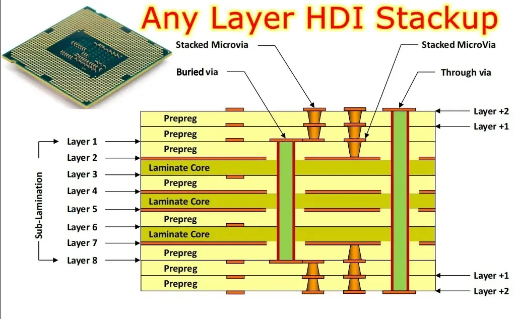
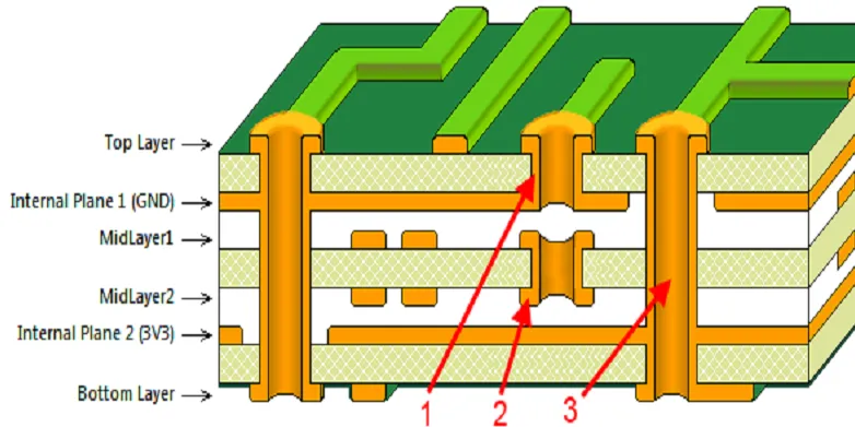
Understanding Blind and Buried Vias in HDI Design
Two key types of microvias used in HDI assembly are blind vias and buried vias. Each serves a unique purpose in optimizing board space and performance during the HDI manufacturing process.
Blind Via Formation
Blind vias connect an outer layer of the PCB to one or more inner layers but do not pass through the entire board. This design saves space on the opposite side of the board, allowing for more routing options. Blind via formation is often used in HDI designs with fine-pitch components like Ball Grid Arrays (BGAs), where space is limited.
The process of creating blind via typically involves laser drilling to achieve precise depths, often as shallow as 50-100 micrometers. Controlling the depth is critical to avoid damaging underlying layers, and modern laser systems can achieve tolerances as tight as ±10 micrometers.
Buried Via Formation
Buried vias, on the other hand, connect internal layers of the PCB without reaching the outer surfaces. This type of via is "buried" within the board, making it invisible from the outside. Buried via formation is ideal for freeing up surface space on both sides of the PCB, enabling more complex routing and component placement.
Creating buried vias often requires a sequential lamination process, where layers are built up step by step, and laser drilling is performed at specific stages. This adds complexity to the HDI manufacturing process but is necessary for advanced designs requiring high layer counts (often 8-12 layers or more in HDI boards).
The Role of Laser Drilling in HDI Microvia Formation
Laser drilling has become the go-to method for laser drilling HDI microvias due to its precision and flexibility. Unlike mechanical drilling, which struggles with holes smaller than 200 micrometers, laser drilling can create vias as small as 25-50 micrometers in diameter. This capability is crucial for HDI assembly, where space is at a premium.
How Laser Drilling Works
Laser drilling uses focused beams of light to vaporize material and create holes in the PCB substrate. The process is highly controlled, with parameters like pulse duration, energy level, and beam focus adjusted to match the material and desired via size. Common laser types include CO2 lasers for larger vias and UV lasers for finer, high-precision work.
For example, a typical CO2 laser system might operate at a wavelength of 10.6 micrometers, suitable for drilling through dielectric materials like FR-4 or polyimide at speeds of up to 1000 vias per second. UV lasers, with wavelengths around 355 nanometers, offer even tighter control for microvias in advanced HDI designs, minimizing thermal damage to surrounding areas.
Advantages of Laser Drilling in HDI Assembly
The benefits of laser drilling HDI are numerous:
- Precision: Laser drilling systems can achieve via aspect ratios (depth-to-diameter) of up to 1:1, ensuring reliable connections in thin layers.
- Speed: Automated laser drilling can process thousands of vias per minute, boosting production efficiency.
- Flexibility: Lasers can drill through a variety of materials, including copper, dielectric, and reinforced laminates, without tool wear.
- Reduced Signal Loss: Smaller vias created by lasers minimize parasitic capacitance and inductance, improving signal integrity at high frequencies (e.g., above 1 GHz).
Key Steps in the HDI Manufacturing Process for Microvia Formation
The HDI manufacturing process is a complex, multi-step journey that requires precision at every stage to ensure reliable microvia formation. Below, we outline the key steps involved when using laser drilling techniques.
1. Design and Planning
Before manufacturing begins, engineers must design the PCB layout, specifying the placement and type of microvias (blind or buried). Design software helps simulate signal performance and ensure impedance control, often targeting values like 50 ohms for high-speed signals. Via sizes, stack-up configurations, and layer counts are finalized at this stage.
2. Material Selection
HDI boards often use thin dielectric materials (e.g., 50-100 micrometers thick) to support microvias. The choice of material impacts laser drilling parameters, as different substrates absorb laser energy differently. For instance, glass-reinforced materials may require slower drilling speeds to avoid cracking.
3. Laser Drilling for Microvias
Once the layers are prepared, laser drilling creates the microvias. For blind vias, the laser stops at a specific depth, often controlled by real-time feedback systems. Buried vias are drilled before additional layers are laminated over them. Post-drilling, the vias are cleaned to remove debris and ensure smooth walls for plating.
4. Via Metallization
After drilling, the microvias are plated with copper to establish electrical connections. Electroless copper deposition followed by electroplating ensures uniform coverage, even in high-aspect-ratio vias. Typical PCB copper thickness in microvias ranges from 15-25 micrometers to balance conductivity and space constraints.
5. Lamination and Testing
For multilayer HDI boards, lamination bonds the layers together under heat and pressure. Sequential lamination may be used for buried vias, adding layers one at a time. Finally, the board undergoes electrical testing to verify connectivity and impedance, ensuring values stay within ±10% of the design target.
Challenges in Microvia Formation and How to Overcome Them
While laser drilling offers unmatched precision for HDI assembly microvia formation, it comes with challenges that manufacturers must address to ensure quality and reliability.
Thermal Damage
Laser drilling generates heat, which can damage delicate materials or cause delamination in multilayer boards. Using UV lasers with shorter pulse durations (e.g., picosecond or femtosecond pulses) minimizes heat-affected zones, reducing damage to less than 10 micrometers around the via.
Via Wall Quality
Rough or uneven via walls can lead to poor copper plating and unreliable connections. Optimizing laser parameters, such as reducing energy density to 5-10 J/cm2 for certain materials, helps achieve smoother walls. Post-drilling cleaning with plasma or chemical desmear processes further improves quality.
Alignment Accuracy
In HDI designs with multiple layers, aligning microvias precisely is critical. Misalignment by even 20 micrometers can cause connection failures. Advanced laser systems with vision-based alignment can achieve accuracies of ±5 micrometers, ensuring proper layer-to-layer registration.
Best Practices for Laser Drilling in HDI Assembly
To achieve optimal results in laser drilling HDI, follow these best practices:
- Choose the Right Laser Type: Use CO2 lasers for cost-effective drilling of larger microvias (75-150 micrometers) and UV lasers for finer vias (below 50 micrometers).
- Optimize Drilling Parameters: Adjust pulse energy, repetition rate, and focus to match the material properties, preventing overheating or incomplete drilling.
- Implement Quality Control: Use automated optical inspection (AOI) to check via dimensions and alignment after drilling, ensuring defects are caught early.
- Collaborate with Manufacturers: Work closely with your PCB fabrication partner to align design specifications with manufacturing capabilities, especially for complex blind via formation or buried via formation.
Future Trends in HDI Microvia Formation
As electronics continue to shrink and performance demands grow, the HDI manufacturing process is evolving. Emerging trends in microvia formation include:
- Smaller Vias: Research is pushing via diameters below 20 micrometers, requiring even more advanced laser technologies.
- Hybrid Drilling: Combining laser and mechanical drilling for cost-effective production of mixed via sizes in HDI boards.
- Automation: AI-driven laser systems are improving drilling accuracy and speed, reducing human error in high-volume production.
Conclusion: Elevate Your HDI Assembly with Laser Drilling Expertise
Mastering HDI PCB assembly microvia formation through laser drilling HDI techniques is essential for producing high-performance, compact PCBs. By understanding the nuances of blind via formation, buried via formation, and the broader HDI manufacturing process, engineers can design and manufacture boards that meet the stringent demands of modern electronics.
Laser drilling stands out as the most effective method for creating precise, reliable microvias, offering unmatched speed and flexibility. By adopting best practices and staying ahead of emerging trends, you can ensure your HDI projects achieve optimal results. Whether you're working on consumer electronics, automotive systems, or medical devices, the insights shared in this guide can help you navigate the complexities of HDI assembly with confidence.


