 ALLPCB


In the world of printed circuit board (PCB) design, managing power distribution is critical for performance and reliability. One technique that often comes up is splitting power planes. But when should you split a power plane, and why does it matter? Simply put, splitting power planes involves dividing a single power layer into multiple sections to isolate different power domains, often to reduce noise and improve signal integrity. This is especially useful in mixed-signal PCBs where analog and digital circuits coexist. In this blog, let's be with ALLPCB to dive deep into the reasons for power plane segmentation, explore split power plane advantages and disadvantages, and guide you on isolating power domains effectively.
What Are Power Planes and Why Do They Matter in PCB Design?
Before we get into splitting power planes, let’s cover the basics. A power plane is a dedicated layer in a multilayer PCB that distributes voltage to various components. Unlike individual traces, a 4 layer PCB power plane provides a low-impedance path for current, ensuring stable power delivery across the board. This reduces voltage drops and minimizes noise, which is essential for high-speed and mixed-signal designs.
Power planes are often paired with ground planes to form a return path for signals, further reducing electromagnetic interference (EMI complaince testing). However, in complex designs with multiple voltage levels or mixed-signal circuits, a single power plane might not be enough. This is where power plane segmentation comes into play.
What Is Power Plane Segmentation?
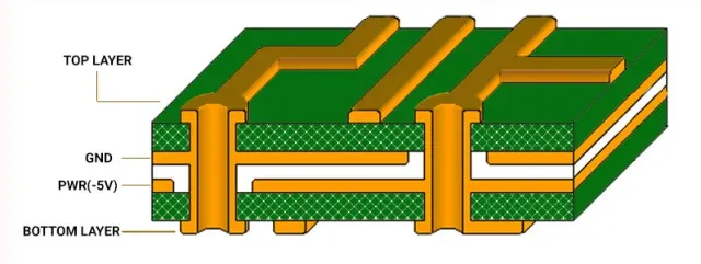
Power plane segmentation, or splitting, refers to dividing a power plane into separate regions to supply different voltages or isolate power domains. For instance, in a mixed-signal PCB, you might have one section of the power plane delivering 3.3V to digital components and another providing 5V to analog circuits. These splits are physically separated by gaps in the copper layer, preventing interference between the domains.
Splitting is often done using isolation techniques like moats (gaps in the plane) or ferrite beads to filter noise between sections. The goal is to keep sensitive circuits, like analog sensors, free from the noise generated by high-speed digital components.
When Should You Consider Splitting Power Planes?
Not every PCB design needs a split power plane. The decision depends on the specific requirements of your project. Here are some common scenarios where splitting is beneficial:
- Mixed-Signal PCBs: When your board includes both analog and digital circuits, splitting the power plane helps isolate noisy digital signals from sensitive analog components. For example, a microcontroller switching at 100 MHz can introduce noise that disrupts a precision analog-to-digital converter (ADC) operating nearby.
- Multiple Voltage Levels: If your design requires different voltages (e.g., 1.8V for low-power components and 5V for others), splitting the power plane ensures each section gets the correct voltage without interference.
- High-Speed Designs: In high-speed circuits, splitting can reduce cross-coupling of noise through the power plane, especially when clock signals exceed 1 GHz. This keeps signal integrity intact.
- Noise-Sensitive Applications: For applications like medical devices or audio equipment, where even small amounts of noise can degrade performance, isolating power domains via splits is often necessary.
Split Power Plane Advantages
Splitting power planes offers several benefits, especially in complex or noise-sensitive designs. Let’s explore the key advantages of this technique:
1. Improved Noise Isolation
One of the biggest reasons for power plane segmentation is to reduce noise. Digital circuits, with their fast-switching signals, generate significant electrical noise that can couple into analog circuits through a shared power plane. By splitting the plane, you create a physical barrier that minimizes this interference. For instance, separating a digital 3.3V domain from an analog 5V domain can reduce noise coupling by up to 20 dB in some designs.
2. Better Signal Integrity
In high-speed designs, maintaining signal integrity is crucial. A split power plane reduces the risk of ground bounce and voltage fluctuations affecting nearby circuits. This is particularly important when dealing with signals faster than 500 MHz, where even small impedance mismatches can cause reflections and data errors.
3. Flexibility for Multiple Voltages
Modern PCBs often require multiple voltage levels to power different components. Splitting the power plane allows you to dedicate specific regions to each voltage, simplifying power distribution. For example, a system-on-chip (SoC) might need 1.2V for its core and 3.3V for I/O pins, and a split plane makes this easy to manage.
4. Reduced EMI
Electromagnetic interference can wreak havoc on PCB performance. By isolating power domains, splitting reduces the spread of EMI across the board. This is especially useful in mixed-signal PCBs, where digital switching noise can radiate and interfere with analog signals if not properly contained.
Split Power Plane Disadvantages
While splitting power planes has clear benefits, it’s not without challenges. Understanding the disadvantages helps you weigh whether this technique is right for your design.
1. Increased Design Complexity
Splitting a power plane adds complexity to the PCB layout. You need to carefully plan the placement of splits, ensure proper routing of traces across gaps, and add filtering components like ferrite beads or decoupling capacitors. This can increase design time and the risk of errors, especially in dense boards.
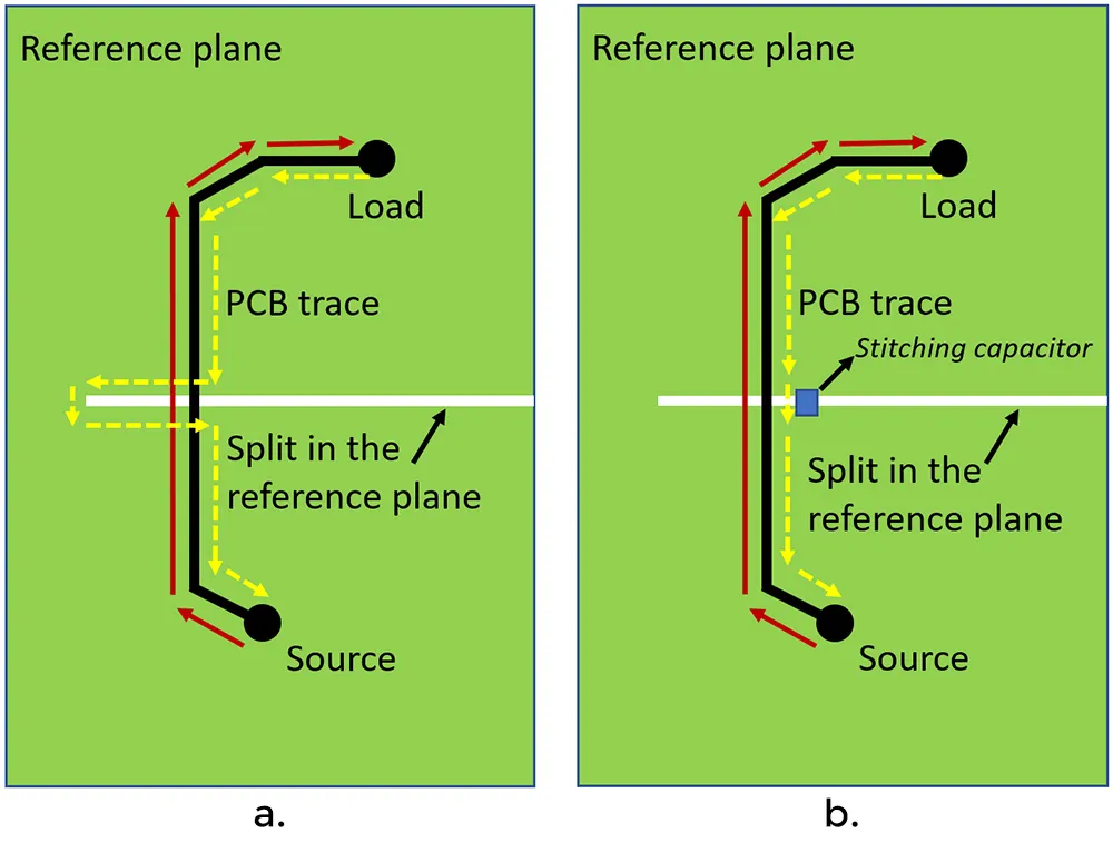
2. Potential for Return Path Issues
When you split a power plane, you also affect the return paths for signals. If a signal trace crosses a split without a nearby ground plane for return current, it can lead to signal integrity issues like crosstalk or increased impedance. For example, a high-speed signal crossing a split might see a return path impedance jump from 50 ohms to over 100 ohms, causing reflections.
3. Higher Manufacturing Costs
Splitting often requires additional layers or more precise manufacturing processes, which can raise custom PCB cost. While a standard four-layer board might suffice for a unified power plane, a split design might need careful alignment of splits and additional vias, increasing fabrication expenses by 10-20% in some cases.
4. Risk of Incomplete Isolation
If not done correctly, splitting can fail to fully isolate noise. For instance, if decoupling capacitors are not placed close enough to components (ideally within 0.1 inches), noise can still couple between domains through parasitic paths. This can negate the benefits of splitting and even worsen performance.
Best Practices for Isolating Power Domains
If you decide to split your power plane, following best practices ensures you maximize the benefits while minimizing drawbacks. Here are actionable tips for isolating power domains effectively:
1. Plan Splits Based on Circuit Layout
Align splits with the natural boundaries of your circuit. For mixed-signal PCBs, place digital components on one side of the split and analog on the other. This minimizes the chance of signals crossing the split and disrupting return paths.
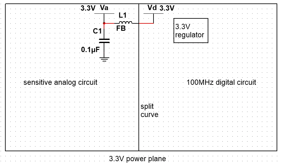
2. Use Filtering Components
To further isolate domains, add ferrite beads or inductors at the boundaries of split planes. These components act as high-frequency filters, blocking noise while allowing DC power to pass. A typical ferrite bead with 600 ohms impedance at 100 MHz can significantly reduce noise coupling.
3. Maintain a Continuous Ground Plane
While splitting power planes is often necessary, avoid splitting the ground plane. A continuous ground plane provides a stable return path for all signals, reducing the risk of EMI and signal integrity issues. If a split ground is unavoidable, ensure it’s done with careful planning and simulation.
4. Place Decoupling Capacitors Strategically
Decoupling capacitors are critical for noise suppression in split designs. Place them as close as possible to the power pins of ICs, ideally within 0.05 to 0.1 inches. Use a mix of capacitance values (e.g., 0.1 μF and 1 μF) to handle a range of frequencies.
5. Simulate and Test Your Design
Before finalizing your PCB, use simulation tools to analyze the impact of splits on signal integrity and noise. Tools can predict impedance mismatches or EMI issues, helping you adjust splits or component placement. Post-fabrication testing with an oscilloscope can also reveal noise levels, ensuring they stay below acceptable thresholds like 50 mV peak-to-peak.
Alternatives to Splitting Power Planes
Splitting isn’t always the best solution. Depending on your design, other techniques might achieve similar results with less complexity. Consider these alternatives:
- Separate Power Supplies: Use dedicated voltage regulators for different domains instead of splitting a single plane. This provides complete isolation without altering the PCB layout.
- Proper Component Placement: Group similar components together (e.g., all digital ICs in one area) to minimize noise coupling, reducing the need for splits.
- Enhanced Decoupling: Use a robust network of decoupling capacitors to suppress noise across a unified power plane, avoiding the need for segmentation.
Conclusion: Is Splitting Power Planes Right for Your Design?
Splitting power planes can be a powerful technique for managing noise and isolating power domains in complex PCB designs, especially in mixed-signal PCBs. The split power plane advantages, like improved noise isolation and better signal integrity, often outweigh the disadvantages when done correctly. However, challenges such as increased design complexity and potential return path issues mean it’s not a one-size-fits-all solution.
By carefully planning splits, using filtering components, and following best practices for isolating power domains, you can ensure your design performs reliably. Whether you’re working on a high-speed system or a noise-sensitive application, understanding when and why to divide your PCB’s power is key to success. Evaluate your project’s needs, simulate potential issues, and choose the approach that balances performance with practicality.
With the right strategy, power plane segmentation can elevate your PCB design, delivering cleaner power distribution and robust operation across diverse applications.


