 ALLPCB


The USB-C connector has revolutionized modern electronics, offering a compact, reversible design capable of delivering high-speed data, power, and versatility in a single package. For engineers designing printed circuit boards (PCBs), integrating USB-C connectors presents both opportunities and challenges. A poorly implemented USB-C design can lead to signal degradation, power delivery issues, or even device failure, while a well-executed one ensures reliability and performance. In this blog, we'll explore practical design guidelines to help you seamlessly integrate USB-C connectors into your PCBs, focusing on signal integrity, power management, and layout best practices. Whether you're working on a consumer gadget or an industrial system, these insights will empower you to create robust, future-proof designs.
USB-C's rise to prominence isn't just about convenience—it's about capability. With support for up to 10 Gbps data transfer (USB 3.1 Gen 2), 100W power delivery, and compatibility with protocols like HDMI and Thunderbolt, it's a game-changer. But with great power comes great responsibility: the dense 24-pin layout and high-speed signals demand precision. Let's dive into the essentials of USB-C PCB integration to ensure your next project performs flawlessly.
Why USB-C Matters for PCB Design
USB-C isn't just another connector—it's a standard that's reshaping how devices connect and communicate. Its reversible plug orientation eliminates user frustration, while its ability to handle high-speed data and substantial power makes it ideal for everything from smartphones to laptops. For PCB designers, this means adapting to tighter tolerances, higher frequencies, and stricter electrical requirements compared to older USB standards like Type-A or Micro-B.
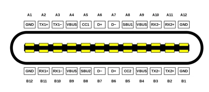
The 24-pin configuration of USB-C includes dedicated lines for USB 2.0 (480 Mbps), USB 3.1 (up to 10 Gbps), power (VBUS and GND), and configuration channels (CC1 and CC2). This complexity requires careful planning to avoid crosstalk, impedance mismatches, and electromagnetic interference (EMI). By following proven design guidelines, you can harness USB-C's full potential while minimizing risks—whether you're aiming for a basic 5V/3A power sink or a high-speed data hub.
Key Design Considerations for USB-C Integration
Signal Integrity: Keeping Data Clean
High-speed signals are the backbone of USB-C's performance, but they're also its Achilles' heel if not handled correctly. The USB 2.0 differential pair (D+ and D-) operates at 480 Mbps, while USB 3.1 SuperSpeed pairs (TX and RX) push up to 10 Gbps. To maintain signal integrity:
- Controlled Impedance: Route differential pairs with a target impedance of 90 ohms (±10%) for USB 3.1 and 85 ohms for USB 2.0. Use a 4-layer PCB with a solid ground plane beneath the traces to achieve this. For example, a trace width of 6 mils and spacing of 8 mils on a 1.6mm FR4 board typically hits this target.
- Length Matching: Keep differential pair lengths within 5 mils (0.127 mm) of each other to avoid timing skew. For USB 3.1, this is critical as signal rise times are as low as 50 ps.
- Minimize Vias and Corners: Each via or sharp turn introduces reflections. Use no more than two vias per differential pair and opt for 45-degree bends instead of 90-degree angles.
Proper routing ensures clean data transmission, reducing bit errors and ensuring compatibility with connected devices.
Recommended Reading: The Impact of Maximum Trace Spacing on Signal Integrity
Power Delivery: Handling Up to 100W
USB-C's Power Delivery (USB PD) spec allows up to 20V at 5A—100W of power—far beyond the 5V/0.5A of early USB standards. This capability demands robust power management:
- VBUS and GND Traces: Use wide traces (at least 20 mils for 3A, scaling to 50 mils for 5A) to handle current without excessive voltage drop or heat. For a 5A design, a 1 oz copper layer should have a trace width of about 40-50 mils to keep temperature rise below 10°C.
- Decoupling Capacitors: Place 0.1 µF and 10 µF capacitors near the VBUS pins to filter noise and stabilize voltage. Position them within 100 mils of the connector for optimal effect.
- CC Pins Configuration: The CC1 and CC2 pins negotiate power roles. For a basic sink (device drawing power), connect 5.1 kΩ pull-down resistors to ground on both CC lines. This signals a 5V/3A capability to the source.
A well-designed power network prevents brownouts and ensures safe operation under load.
Suggested Reading: Calculating PCB Board Power
EMI and Shielding: Reducing Noise
High-speed signals and power switching generate EMI, which can interfere with nearby circuits or violate regulatory standards. Mitigate this with:
- Ground Planes: Surround USB-C traces with a continuous ground plane on adjacent layers. Avoid routing signals over splits or cutouts, which disrupt return paths and increase EMI.
- Shielding: Connect the USB-C connector's metal shell to ground via multiple vias (at least four) to shunt noise. Space these vias evenly around the connector footprint.
- Component Placement: Keep high-speed clocks, oscillators, or magnetic components at least 50 mils away from USB traces to prevent coupling.
Effective EMI control keeps your design compliant and reliable in noisy environments.
Recommended Reading: EMI/EMC Shielding Strategies for Automotive PCBs: Protecting Critical Electronic Systems
PCB Layout Guidelines for USB-C
Connector Placement
Position the USB-C connector near the PCB edge to simplify plug access and minimize trace lengths. For surface-mount connectors, ensure the footprint aligns with manufacturer specs—typically a 0.5mm pitch for pins and a 3.16mm width for the receptacle. Secure it with through-hole mounting tabs for mechanical stability, especially in devices subject to frequent plugging.
Differential Pair Routing
Route USB 2.0 (D+/D-) and USB 3.1 (TX/RX) differential pairs as tightly coupled pairs:
- Space traces 5-8 mils apart within a pair, and at least 20 mils from other signals to reduce crosstalk.
- Avoid running traces under crystals, ICs, or other noisy components. For example, a 25 MHz crystal near a USB 3.1 pair can induce jitter if not isolated.
- Use length tuning (e.g., serpentine traces) to match pair lengths, keeping skew below 5 mils.
Grounding and Layer Stackup
A 4-layer stackup is ideal for USB-C designs:
- Layer 1 (Top): Signal traces and components.
- Layer 2: Solid ground plane.
- Layer 3: Power plane or additional ground.
- Layer 4 (Bottom): Low-speed signals or secondary routing.
For USB 3.1, route SuperSpeed pairs on the top layer over a ground plane on Layer 2. This minimizes impedance discontinuities and provides a low-inductance return path. Add stitching vias along the trace edges every 100-200 mils to tie ground planes together.
Common Pitfalls and How to Avoid Them
Impedance Mismatches
An impedance mismatch—say, 100 ohms instead of 90 ohms—can cause signal reflections, degrading data rates. Use a PCB design tool with an impedance calculator and verify with your fabricator's stackup data. Test a prototype with a time-domain reflectometer (TDR) to confirm.
Overheating Power Traces
Undersized VBUS traces (e.g., 10 mils for 5A) can overheat, risking delamination or failure. Calculate trace width using IPC-2221 standards: for 1 oz copper at 5A, you need at least 47 mils with a 20°C rise. Double-check with a thermal simulation if pushing limits.
Poor ESD Protection
USB-C ports are exposed to electrostatic discharge (ESD). Without protection, a 15 kV strike can fry your ICs. Add ESD suppressors (e.g., TVS diodes rated for 5V or 20V, depending on VBUS) near the connector, within 50 mils of the pins.
Testing Your USB-C Design
Before mass production, validate your PCB:
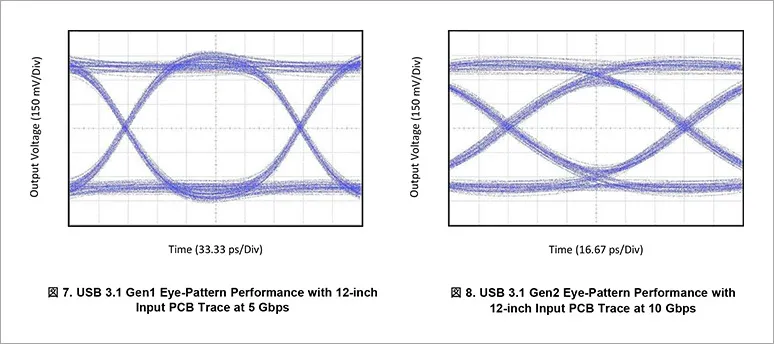
- Signal Integrity Testing: Use an oscilloscope to check eye diagrams for USB 2.0 and 3.1 signals. A clean eye (e.g., >80% height, <20% jitter) confirms compliance.
- Power Delivery: Load test VBUS at max current (e.g., 3A or 5A) and measure voltage drop. It should stay within 5% of the spec (e.g., 4.75V min for 5V).
- Compliance: Run USB-IF certification tests if targeting commercial markets. Tools like the Ellisys USB Explorer can automate this.
Prototyping and iteration catch issues early, saving time and cost.
Leveraging ALLPCB for USB-C Success
For engineers tackling USB-C integration, partnering with a reliable PCB manufacturer can make all the difference.ALLPCB offers pcb prototyping to test your designs in days, not weeks, ensuring you can iterate fast on signal routing or power tweaks. Our advanced manufacturing capabilities support tight tolerances—like 6-mil traces and 0.5mm-pitch footprints—critical for USB-C's dense layout. Plus, with global logistics, we deliver boards wherever your project takes you, keeping your timeline on track. Whether you're refining a high-speed data hub or a rugged power sink, ALLPCB's expertise helps bring your USB-C vision to life.
Conclusion
Integrating USB-C connectors into your PCB design unlocks a world of possibilities—high-speed data, robust power delivery, and universal compatibility. But success hinges on precision: controlled impedance, thoughtful routing, and solid grounding are non-negotiable. By following these guidelines—keeping differential pairs tight, sizing power traces right, and shielding against EMI—you'll build a design that's not just functional but reliable. Test thoroughly, avoid common pitfalls, and you'll have a USB-C implementation that stands up to real-world demands. Ready to start? We're here to help you turn your ideas into reality with confidence.


