 ALLPCB


In the fast-evolving world of automotive technology, electronic systems are at the heart of vehicle safety, performance, and connectivity. However, these critical systems are constantly exposed to electromagnetic interference (EMI), which can disrupt their operation. Ensuring electromagnetic compatibility (EMC) through effective shielding strategies is vital for automotive PCBs (Printed Circuit Boards). This blog dives deep into automotive PCB EMI shielding, EMC compliance PCB techniques, and practical design guidelines to protect critical systems. Whether you're an engineer or a designer, you'll find actionable insights on grounding techniques, filtering techniques, and automotive PCB design guidelines to achieve electromagnetic compatibility.
Why EMI/EMC Shielding Matters for Automotive PCBs
Modern vehicles are packed with electronic control units (ECUs), sensors, infotainment systems, and advanced driver-assistance systems (ADAS). These systems operate in a harsh electromagnetic environment, surrounded by high-power components like electric motors and wireless communication devices. Without proper EMI shielding and EMC compliance, interference can lead to signal distortion, system malfunctions, or even safety hazards. For instance, a disrupted signal in an ADAS module could delay critical braking responses, endangering lives.
EMI shielding prevents external or internal electromagnetic fields from interfering with sensitive circuits, while EMC ensures that a device operates without affecting or being affected by other systems. In automotive applications, achieving both is non-negotiable to meet stringent industry standards like ISO 11452 and CISPR 25, which define acceptable EMI levels for vehicle electronics.

Key Challenges in Automotive PCB EMI/EMC Compliance
Automotive environments present unique challenges for EMI/EMC compliance due to the following factors:
- High-Density Electronics: PCBs in vehicles are often compact, with components packed closely together, increasing the risk of crosstalk and interference.
- Harsh Operating Conditions: Temperature swings, vibrations, and humidity can degrade shielding materials or affect grounding stability.
- Wide Frequency Range: Automotive systems operate across a broad spectrum of frequencies, from low-frequency power systems to high-frequency wireless signals, making EMI control complex.
- Regulatory Standards: Strict EMC standards require extensive testing and design adjustments to ensure compliance.
Addressing these challenges requires a multi-layered approach, combining shielding materials, layout optimization, and robust design practices. Let's explore the most effective strategies for automotive PCB EMI shielding and EMC compliance PCB design.
Effective EMI/EMC Shielding Strategies for Automotive PCBs
1. Use of EMI Shielding Materials and Enclosures
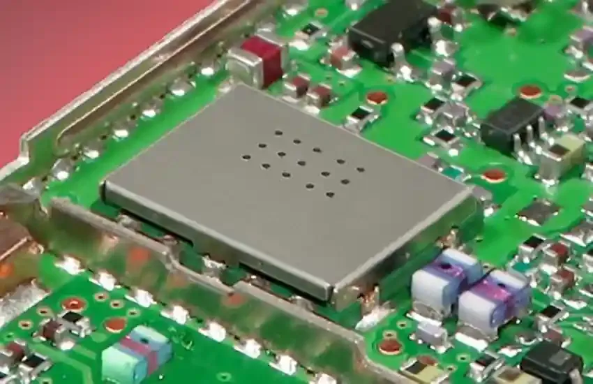
One of the primary methods to protect automotive PCBs from EMI is by using conductive shielding materials. These materials block or redirect electromagnetic fields, preventing them from reaching sensitive components. Common options include:
- Metal Shields: Aluminum or copper shields can be placed over critical components to block external EMI. These are often lightweight and cost-effective for automotive applications.
- Conductive Coatings: Applying conductive paints or coatings to PCB enclosures can provide an additional layer of protection against high-frequency interference.
- Gaskets and Seals: Conductive gaskets ensure that enclosures remain EMI-tight by sealing gaps where electromagnetic waves could penetrate.
For example, a metal shield over a high-frequency RF module can reduce interference by up to 30 dB, significantly improving signal integrity. However, ensure that the shielding material is compatible with the vehicle's thermal and mechanical requirements to avoid degradation over time.
2. Grounding Techniques for EMI Reduction
Proper grounding techniques are essential for minimizing EMI and ensuring electromagnetic compatibility. Grounding provides a low-impedance path for unwanted currents to dissipate, reducing noise in the system. Key grounding strategies include:
- Single-Point Grounding: Connect all ground points to a single reference to avoid ground loops, which can act as antennas for EMI. This is particularly effective for low-frequency systems.
- Multi-Layer Ground Planes: In multi-layer PCBs, dedicate an entire layer to ground. A solid ground plane with an impedance of less than 1 ohm can significantly reduce noise coupling between traces.
- Ground Stitching Vias: Use multiple vias to connect ground planes across layers, ensuring a consistent low-impedance path. Space vias at intervals of less than λ/20 (where λ is the wavelength of the highest frequency signal) to prevent EMI leakage.
In automotive PCBs, grounding must also account for the vehicle's chassis, which often serves as a common ground. Ensure secure connections to the chassis to avoid floating grounds, which can amplify interference.
3. Filtering Techniques to Suppress EMI
Filtering techniques are critical for suppressing EMI at the source or preventing it from reaching sensitive circuits. Filters remove unwanted frequencies while allowing desired signals to pass. Common filtering methods include:
- Low-Pass Filters: These are used to block high-frequency noise in power lines. For instance, a low-pass filter with a cutoff frequency of 100 kHz can effectively reduce switching noise from power converters.
- Ferrite Beads: Placed in series with power traces, ferrite beads act as high-frequency chokes, attenuating noise above 10 MHz while allowing DC current to flow.
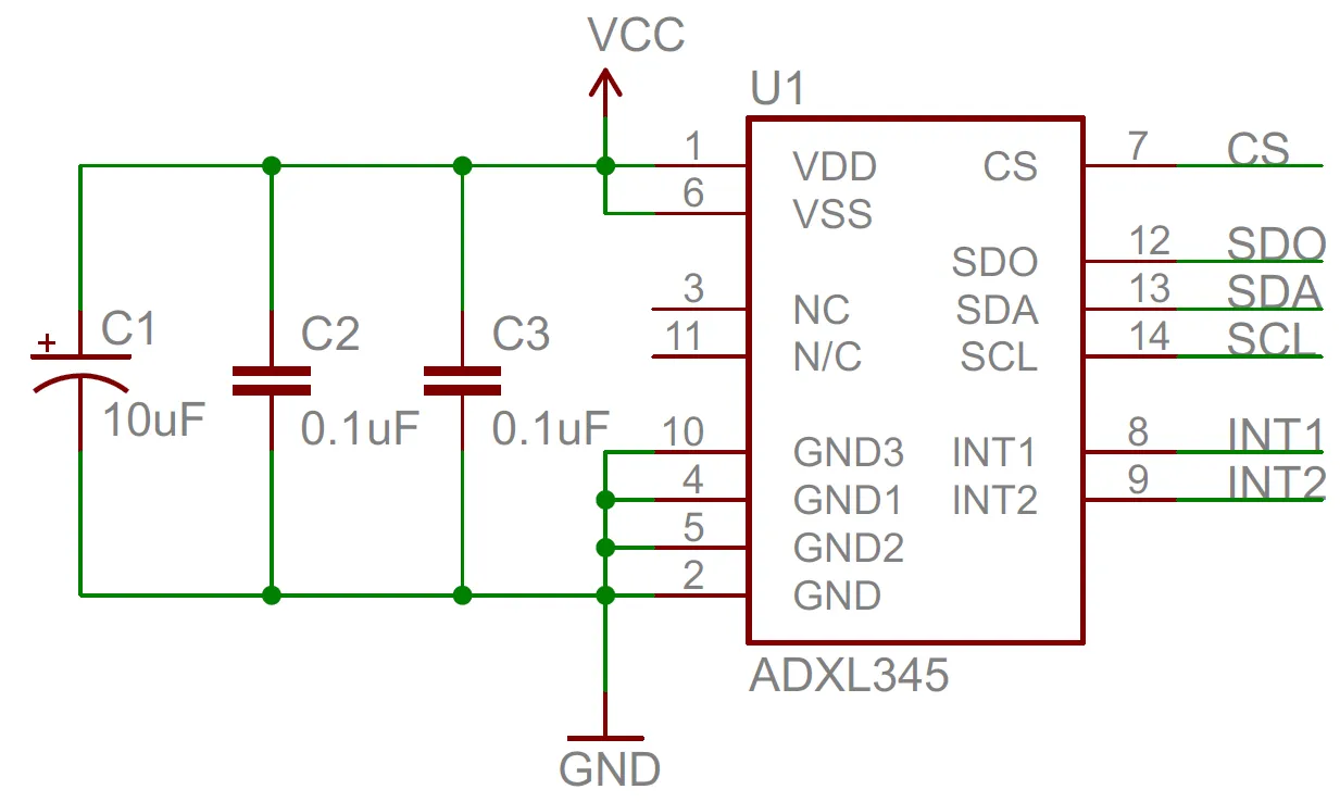
- Decoupling Capacitors: Positioned close to IC power pins, these capacitors (typically 0.1 μF to 1 μF) shunt high-frequency noise to ground, stabilizing voltage levels.
In automotive designs, filters must be selected based on the operating frequency of the system. For example, in a CAN bus system operating at 1 Mbps, ensure that filters do not attenuate signals below 5 MHz to avoid data loss.
4. Automotive PCB Design Guidelines for EMC Compliance
Designing for EMC compliance PCB starts at the layout stage. Poor layout choices can amplify EMI, even with the best shielding materials. Follow these automotive PCB design guidelines to minimize interference:
- Trace Separation: Keep high-speed signal traces (e.g., clock lines) away from power traces to prevent crosstalk. Maintain a spacing of at least 3 times the trace width for signals operating above 50 MHz.
- Short Trace Lengths: Minimize the length of high-frequency traces to reduce their ability to act as antennas. For signals above 100 MHz, keep trace lengths below 1/10th of the wavelength.
- Component Placement: Group noisy components (like switching regulators) away from sensitive analog circuits. Place decoupling capacitors within 1 cm of IC power pins to maximize effectiveness.
- Layer Stackup: Use a 4-layer or higher PCB stackup with dedicated power and ground planes. A typical stackup might be Signal-Ground-Power-Signal, ensuring that high-speed signals are routed adjacent to a ground plane for controlled impedance.
By adhering to these guidelines, designers can reduce EMI by up to 20 dB, significantly improving system reliability in automotive environments.
Testing and Validation for EMC Compliance in Automotive PCBs
Designing for EMI/EMC is only half the battle; rigorous testing is essential to ensure compliance with automotive standards. Common tests include:
- Radiated Emissions Testing: Measures the electromagnetic fields emitted by the PCB, ensuring they fall within limits defined by CISPR 25 (typically below 30 dBμV/m at 1 meter for frequencies up to 1 GHz).
- Conducted Emissions Testing: Evaluates noise conducted through power lines, often requiring levels below 50 dBμV in the 150 kHz to 30 MHz range.
- Immunity Testing: Exposes the PCB to external EMI (per ISO 11452) to verify that it operates without failure under field strengths up to 100 V/m.
Testing should be conducted early in the design phase using pre-compliance tools to identify issues before full certification. This iterative approach saves time and cost, ensuring that the final design meets all regulatory requirements for electromagnetic compatibility.
Future Trends in Automotive PCB EMI/EMC Shielding
As vehicles become more electrified and connected, EMI/EMC challenges will intensify. Emerging trends include:
- Electric Vehicle (EV) Powertrains: High-voltage systems in EVs generate significant EMI, requiring advanced shielding and filtering solutions to protect low-voltage control circuits.
- 5G Integration: The adoption of 5G for vehicle-to-everything (V2X) communication introduces high-frequency EMI, necessitating tighter layout controls and shielding at frequencies up to 6 GHz.
- Advanced Materials: Lightweight, flexible shielding materials like conductive polymers are gaining traction for their ability to conform to complex PCB geometries without adding weight.
Staying ahead of these trends requires continuous learning and adaptation of design practices to address new EMI sources and compliance requirements.
Conclusion: Building Reliable Automotive PCBs with EMI/EMC Shielding
Protecting critical electronic systems in vehicles starts with robust EMI/EMC shielding strategies. By leveraging effective automotive PCB EMI shielding, implementing grounding techniques, applying filtering techniques, and following automotive PCB design guidelines, engineers can ensure electromagnetic compatibility and meet stringent industry standards. A well-designed PCB not only enhances system reliability but also contributes to passenger safety and vehicle performance.
At ALLPCB, we’re committed to supporting engineers with the tools and resources needed to design high-quality automotive PCBs. From prototyping to production, our services help you navigate the complexities of EMC compliance PCB requirements. Start your next project with confidence, knowing that your designs are built to withstand the toughest electromagnetic challenges.





