ALLPCB


SK Hynix is advancing hybrid bonding technology for high-bandwidth memory (HBM), with plans to implement it first in HBM4E, currently in the research and development phase. This move aligns with customer demands for increased bandwidth, improved power efficiency, and higher integration in memory solutions.
Hybrid Bonding: Meeting Industry Needs
Hybrid bonding addresses key requirements for next-generation memory by enabling higher stack layers and thicker dies, improving warpage issues compared to traditional microbump stacking. By bonding chips using dielectric materials like silicon dioxide with embedded copper contacts, followed by thermal processing to expand and connect the copper, hybrid bonding eliminates bumps, allowing tighter interconnect pitches (10 ¦Ìm or less). This results in faster data transfer rates and better thermal performance.
Applications Beyond HBM
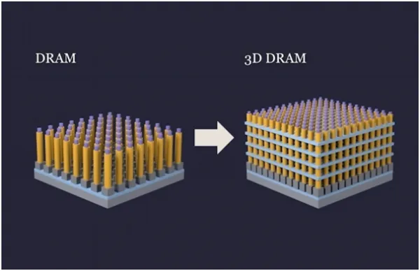
Beyond HBM, hybrid bonding shows promise for 3D DRAM and NAND flash. By separately fabricating DRAM cell and peripheral regions and bonding them using a 3D structure, hybrid bonding can overcome the miniaturization limits of 2D DRAM. Similarly, NAND flash can leverage this technology to increase layer counts, enhancing storage density. For instance, Yangtze Memory¡¯s Xtacking hybrid bonding technology has enabled its fifth-generation 3D TLC NAND flash with 294 layers, including 232 active layers, achieving the highest storage density among commercial 3D NAND products.
SK Hynix¡¯s HBM4 and HBM4E Roadmap
SK Hynix plans to mass-produce 12-layer HBM4 in 2025 and supply HBM4E based on customer needs, reinforcing its leadership in the HBM market. The company¡¯s 1c nm DRAM process, with yields recently improved to approximately 80%, is nearing the 80¨C90% threshold required for full-scale production. This process will support HBM4E using 32 Gb DRAM dies, alongside other advanced DRAM products like LPDDR6 and GDDR7, offering high performance and cost competitiveness.
Industry-Wide Adoption of Hybrid Bonding
Major HBM manufacturers are expected to fully adopt hybrid bonding by the HBM5 20-layer generation to address stack height limits, I/O density, and thermal challenges. SK Hynix is exploring hybrid bonding as a strategic option for HBM4E, while Samsung has confirmed its use for HBM4 to enhance thermal and interface performance. Meanwhile, Yangtze Memory¡¯s Xtacking patents have gained traction, with Samsung securing a licensing agreement for its next-generation (V10) NAND flash, targeting 420¨C430 layers by late 2025. SK Hynix may also pursue similar agreements for its 400+ layer NAND development.
Conclusion
Hybrid bonding is poised to transform memory technologies, starting with HBM4E and extending to 3D DRAM and NAND flash. SK Hynix¡¯s advancements in HBM4 and HBM4E, coupled with its 1c nm process and potential adoption of hybrid bonding, position it to meet the growing demands of AI and high-performance computing. As the industry moves toward higher integration and efficiency, hybrid bonding will play a critical role in overcoming the limitations of traditional stacking methods.