 ALLPCB


Are you looking to understand the ins and outs of flexible PCB manufacturing? Flexible PCBs, also known as flex circuit boards, are essential in modern electronics, offering unique design freedom for compact and lightweight applications. In this comprehensive guide, we’ll walk you through the detailed process of flexible PCB production, from raw materials to the final product, ensuring you have a clear picture of PCB fabrication. Whether you’re an engineer, designer, or manufacturer, this step-by-step explanation of the PCB manufacturing process will help you navigate the world of flex circuit boards with confidence.
What Are Flexible PCBs and Why Are They Important?
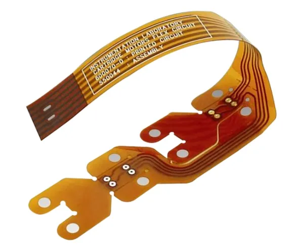
Flexible PCBs are printed circuit boards made from flexible materials like polyimide (PI) or polyester, allowing them to bend, fold, and twist without breaking. Unlike rigid PCBs, flex circuit boards are ideal for applications where space and weight are critical, such as in smartphones, wearable devices, medical equipment, and aerospace systems. Their ability to conform to unique shapes makes them a go-to solution for innovative product designs.
The importance of flexible PCB production lies in its ability to enable smaller, lighter, and more durable electronics. With the rise of compact devices, understanding the PCB manufacturing process for flex boards is crucial for staying competitive in the electronics industry. Let’s dive into the detailed steps of PCB fabrication for flexible circuits.
Overview of the Flexible PCB Manufacturing Process
The PCB manufacturing process for flexible circuits involves multiple stages, each critical to ensuring the final product meets design and performance standards. While the process shares similarities with rigid PCB fabrication, the materials and techniques used in flexible PCB production require specialized handling. Below, we break down the step-by-step guide to creating high-quality flex circuit boards.
Step 1: Design and Layout Creation
The first step in flexible PCB production is designing the circuit layout. Engineers use advanced software to create a digital blueprint of the PCB, defining the placement of components, traces, and vias. This design must account for the bending and folding requirements of the final application to avoid stress on critical areas.
Key considerations during design include trace width (often as small as 0.003 inches or 75 micrometers for high-density designs) and spacing to ensure signal integrity. Impedance control is also vital, with typical values ranging from 50 to 100 ohms for high-speed signals in flex circuits. Once the design is finalized, it’s converted into Gerber files, which serve as instructions for the manufacturing equipment.
Step 2: Material Selection
Material choice is a cornerstone of the PCB manufacturing process for flex circuit boards. The most common base material is polyimide (PI), known for its high thermal stability (up to 260°C) and flexibility. Polyester is another option for less demanding applications due to its lower cost but reduced heat resistance.
Copper foil, typically 0.5 to 2 ounces per square foot (17 to 70 micrometers thick), is laminated onto the base material as the conductive layer. Adhesives or adhesive-less bonding techniques are used to secure the layers, depending on the design requirements. The choice of materials directly impacts the durability and performance of the flex PCB during use.
Step 3: Lamination and Layer Bonding
Once materials are selected, the next step in PCB fabrication is lamination. This process bonds the copper foil to the flexible substrate using heat and pressure. For multilayer flex circuit boards, multiple layers of copper and substrate are stacked and bonded together. Precision is key to avoid misalignment, which can lead to signal loss or failure.
In adhesive-less lamination, often used for thinner designs, the copper is directly bonded to the substrate, reducing thickness (down to 0.002 inches or 50 micrometers per layer) and improving flexibility. This step sets the foundation for the circuit’s structure and must be done with exact control over temperature and pressure.
Step 4: Circuit Patterning (Photolithography)
With the layers bonded, the circuit pattern is transferred onto the copper using a process called photolithography. A photoresist layer is applied to the copper surface, and the Gerber file design is projected onto it using UV light. Areas exposed to light harden, while unexposed areas are washed away, leaving a mask of the desired circuit pattern.
The exposed copper is then etched away using a chemical solution, typically ferric chloride, revealing the traces and pads. This step is critical in flexible PCB production as it defines the electrical pathways. Trace widths as narrow as 0.002 inches (50 micrometers) can be achieved for high-density interconnects.
Step 5: Drilling and Via Formation
For multilayer flex circuit boards, vias (small holes) are drilled to connect different layers. Laser drilling is often used due to its precision, creating holes as small as 0.001 inches (25 micrometers) in diameter. These vias are later plated with copper to ensure electrical conductivity between layers.
In flexible PCBs, drilling must be done carefully to avoid damaging the thin, delicate materials. Misaligned or oversized vias can weaken the board or disrupt signal paths, so advanced equipment with tight tolerances is essential.
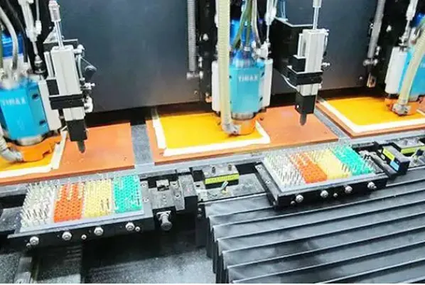
Step 6: Copper Plating and Surface Finishing
After drilling, the vias and exposed copper areas are plated with a thin layer of copper to ensure connectivity. This is typically done through an electroplating process, adding a layer of copper about 0.001 inches (25 micrometers) thick. A surface finish, such as Electroless Nickel Immersion Gold (ENIG), is then applied to protect the copper from oxidation and improve solderability.
ENIG finishes are popular in flexible PCB production because they provide a flat surface and withstand multiple bending cycles without cracking. The thickness of the gold layer is usually 0.000002 to 0.000008 inches (0.05 to 0.2 micrometers), balancing cost and performance.
Step 7: Coverlay Application
Unlike rigid PCBs that use solder masks, flex circuit boards often use a coverlay—a flexible insulating film—to protect the circuit. The coverlay, typically made of polyimide with an adhesive layer, is laminated over the board, leaving openings for pads and components. This layer adds durability and protects against environmental factors like moisture and dust.
The coverlay thickness usually ranges from 0.001 to 0.002 inches (25 to 50 micrometers), ensuring the board remains flexible while providing adequate insulation. Precision alignment during application is crucial to avoid covering critical connection points.
Step 8: Cutting and Profiling
Once the circuit is fully formed, the flexible PCB is cut into its final shape. This can be done using laser cutting for high precision or mechanical die-cutting for larger volumes. The profiling process ensures the board fits perfectly into the intended application, whether it’s a curved wearable device or a compact medical sensor.
Laser cutting is often preferred in flexible PCB production as it minimizes stress on the material, preventing tears or cracks. Tolerances as tight as ±0.002 inches (±50 micrometers) are achievable, ensuring a perfect fit.
Step 9: Testing and Quality Assurance
Quality control is a vital part of the PCB manufacturing process. Each flexible PCB undergoes rigorous testing to ensure functionality and reliability. Electrical tests check for continuity and shorts, while impedance testing verifies signal integrity, often targeting values between 50 and 100 ohms for high-speed applications.
Flex cycle testing is also performed to simulate bending and folding, ensuring the board can withstand thousands of cycles (often 10,000 or more) without failure. Visual inspections and automated optical inspection (AOI) systems detect any surface defects or misalignments before the boards are shipped.
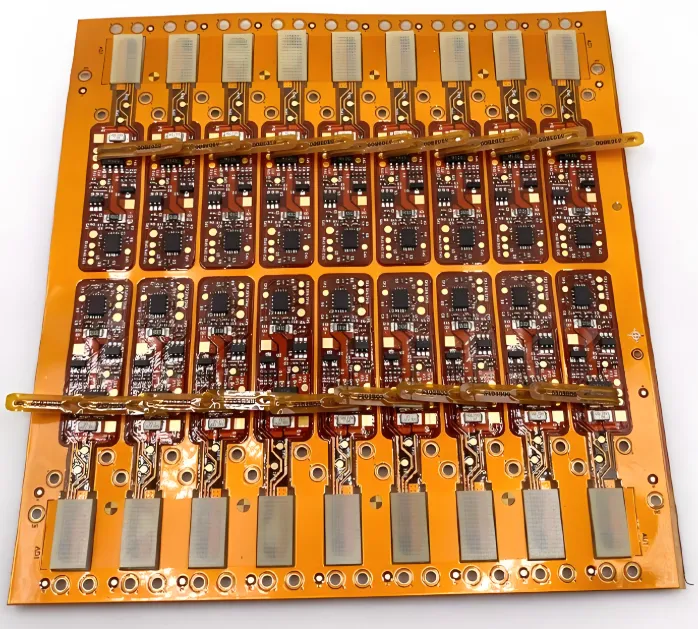
Step 10: Assembly and Final Integration
The final step in flexible PCB fabrication is assembly, where components are mounted onto the board. Surface-mount technology (SMT) is commonly used due to the compact nature of flex circuits. Soldering must be done at controlled temperatures (typically below 260°C for polyimide substrates) to avoid damaging the flexible material.
After assembly, the flex circuit board is integrated into the final product, whether it’s a foldable smartphone or a medical implant. Proper handling during integration is critical to prevent stress on the board and ensure long-term reliability.
Suggested Reading: Mastering SMT Assembly on Flexible Boards: Techniques and Best Practices
Benefits of Flexible PCBs in Modern Applications
Understanding the PCB manufacturing process for flex circuit boards highlights why they are so valuable. Here are some key benefits:
- Space and Weight Savings: Flex PCBs reduce the need for connectors and cables, saving up to 60% of space and weight compared to rigid boards.
- Durability: They can endure dynamic flexing, with some designs tested for over 200,000 bend cycles.
- Design Freedom: Their ability to conform to 3D shapes allows for innovative product designs in industries like wearables and aerospace.
- Reliability: Fewer interconnects mean fewer points of failure, improving overall system reliability.
Challenges in Flexible PCB Production
While the benefits are clear, flexible PCB production comes with challenges. The materials are more expensive than those used in rigid PCBs, with polyimide costing up to 30% more than standard FR-4. The manufacturing process also requires specialized equipment and expertise, increasing production costs.
Additionally, designing for flexibility demands careful planning to avoid stress points that could lead to cracking or delamination. Engineers must balance performance with manufacturability, ensuring the design can be produced at scale without defects.
Tips for Successful Flexible PCB Fabrication
To achieve optimal results in flexible PCB manufacturing, consider the following tips:
- Collaborate closely with your manufacturer during the design phase to ensure compatibility with their processes.
- Specify bending requirements upfront, including minimum bend radius (often 6-10 times the board thickness for polyimide).
- Opt for adhesive-less lamination for thinner, more flexible designs if your application allows.
- Prioritize testing for flex cycles and environmental resistance to guarantee long-term performance.
Conclusion: Mastering Flexible PCB Manufacturing
Flexible PCB production is a complex but rewarding process that powers some of the most innovative electronics today. By understanding each step of the PCB manufacturing process—from design and material selection to testing and assembly—you can ensure high-quality flex circuit boards that meet the demands of your application. Whether you’re working on a wearable device, medical equipment, or aerospace system, mastering PCB fabrication for flexible circuits opens up a world of design possibilities.
At ALLPCB, we’re committed to supporting your journey through every stage of flexible PCB manufacturing. With expertise in producing high-quality flex circuit boards, we’re here to help bring your ideas to life with precision and reliability. Dive into the world of flexible PCB production and see how these innovative boards can transform your next project.


