 ALLPCB


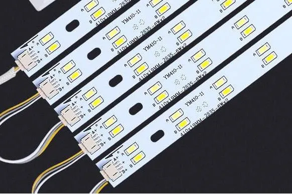
LED lighting has revolutionized the way we illuminate our world, offering energy efficiency and long-lasting performance. However, one critical challenge in LED PCB design is managing heat. High-power LEDs generate significant heat, and without proper thermal management for LEDs, their efficiency drops, and their lifespan shortens. This is where thermal vias come into play. These small, heat-conducting pathways in LED PCBs help dissipate heat, ensuring your LEDs stay cool and perform optimally.
In this blog, let's be with ALLPCB to dive deep into the role of thermal vias in LED cooling techniques, explore their importance in high-power LED PCBs, and provide practical tips for incorporating them into your designs. Whether you're an engineer or a designer working on cutting-edge lighting solutions, you'll find actionable insights to improve your projects.
Why Thermal Management for LEDs Matters
LEDs, especially high-power ones, convert a significant portion of electrical energy into heat—often around 70%, with only 30% becoming light, according to widely available data on the web. If this heat isn't managed, the LED junction temperature rises, leading to reduced light output, color shifts, and even premature failure. For instance, operating an LED above its maximum junction temperature (often around 120-150°C for many models) can cut its lifespan from 50,000 hours to just a fraction of that.
Effective thermal management for LEDs ensures that the heat is moved away from the LED chip to a heat sink or the surrounding environment. This not only maintains efficiency but also guarantees reliability in applications like automotive lighting, streetlights, and industrial illumination. Without a solid strategy for LED cooling, even the best designs can underperform.
Suggested Reading: The Ultimate Guide to Thermal Via Placement: Cooling Your PCB Effectively
What Are Thermal Vias and How Do They Work?
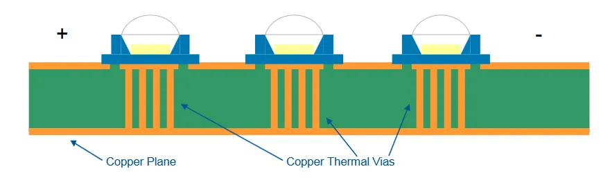
Thermal vias are small, copper-filled or copper-plated holes in a PCB that act as pathways for heat to travel from the LED component to a heat-dissipating layer, such as a ground plane or heat sink. Unlike regular vias used for electrical connections, thermal vias are specifically designed to enhance heat transfer in high-power LED PCBs.
Here’s how they work: Heat generated by the LED flows into the PCB through the component's thermal pad. Thermal vias, placed directly under or near the LED, provide a low-resistance path for this heat to move to the bottom layer of the PCB or other heat-dissipating structures. Typically, these vias are filled with a conductive material like copper to maximize thermal conductivity, which can be as high as 400 W/m·K for pure copper.
In LED PCB design, thermal vias are often arranged in an array beneath the LED to ensure even heat distribution. Their effectiveness depends on factors like the number of vias, their diameter (commonly 0.3-0.5 mm), and the thickness of the copper layers (often 1-2 oz per square foot).
The Benefits of Using Thermal Vias in LED Cooling Techniques
Incorporating thermal vias into your LED PCB design offers several advantages, especially for high-power applications. Here are some key benefits:
- Improved Heat Dissipation: Thermal vias reduce the thermal resistance between the LED and the heat sink, lowering junction temperatures by as much as 10-20°C in some designs, depending on the layout and materials used.
- Enhanced LED Lifespan: By keeping temperatures low, thermal vias help maintain the LED’s rated lifespan, often extending it beyond 50,000 hours under optimal conditions.
- Better Efficiency: Cooler LEDs operate more efficiently, maintaining consistent light output and color accuracy over time.
- Compact Design Compatibility: Thermal vias allow for smaller PCB layouts by efficiently managing heat without requiring bulky external cooling solutions.
For example, in a high-power LED streetlight design, using an array of thermal vias can prevent overheating even when the ambient temperature reaches 40°C or higher, ensuring reliable performance in harsh conditions.
Design Considerations for Thermal Vias in High-Power LED PCBs
While thermal vias are a powerful tool for LED cooling techniques, their effectiveness depends on thoughtful design. Below are some critical factors to consider when integrating them into your LED PCB design:
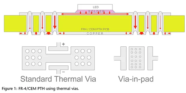
1. Placement and Layout
Position thermal vias directly beneath or as close as possible to the LED’s thermal pad. A grid or array pattern often works best, with 8-16 vias per LED for high-power applications. Spacing should be tight enough to maximize heat transfer but not so dense that it compromises the structural integrity of the PCB. A common spacing is around 1-1.5 mm between vias.
2. Via Size and Fill Material
Via diameter typically ranges from 0.3 to 0.5 mm for thermal applications. Smaller vias allow for more to be placed in a given area, but larger vias can transfer heat more effectively if filled with copper. Copper-filled vias are preferred over unfilled or epoxy-filled ones because of copper’s superior thermal conductivity.
3. Copper Layer Thickness
The thickness of the copper layers connected by thermal vias plays a big role in heat dissipation. A thicker copper layer, such as 2 oz/ft2, can spread heat more effectively across the PCB compared to a standard 1 oz/ft2 layer. For high-power LED PCBs, consider using heavier copper for better results.
4. Connection to Heat Sinks or Ground Planes
Thermal vias should connect to a large copper plane or heat sink on the opposite side of the PCB. This plane acts as a heat spreader, distributing thermal energy over a wider area for dissipation. Ensure the connection is direct and uninterrupted by other components or traces.
Other LED Cooling Techniques to Complement Thermal Vias
While thermal vias are essential for PCB thermal management for LEDs, they work best when combined with other cooling strategies. Here are some additional techniques to consider for high-power LED PCBs:
1. Metal Core PCBs (MCPCBs)
Metal core PCBs use a metal base, often aluminum, instead of the standard FR4 material. This metal layer acts as a built-in heat sink with thermal conductivity up to 200 W/m·K, far higher than FR4’s 0.3 W/m·K. Combining MCPCBs with thermal vias can significantly enhance heat dissipation.
2. Heat Sinks and Fans
Attaching a heat sink to the PCB provides a large surface area for heat to dissipate into the air. For applications with extreme heat, active cooling with fans can further improve performance. Ensure thermal vias are aligned with the heat sink attachment points for maximum efficiency.
3. Thermal Interface Materials (TIMs)
Using high-quality thermal interface materials between the LED and PCB, or between the PCB and heat sink, reduces thermal resistance. TIMs like thermal paste or pads can improve heat transfer by filling microscopic gaps, with thermal conductivity ranging from 1 to 8 W/m·K depending on the material.
4. Optimized Component Placement
Space out heat-generating components on the PCB to avoid creating hot spots. Place LEDs away from other high-power elements if possible, and ensure thermal vias have clear paths to dissipate heat without interference from nearby traces.
Common Challenges with Thermal Vias and How to Overcome Them
While thermal vias are highly effective, they come with some challenges in LED PCB design. Here’s how to address them:
- Manufacturing Costs: Copper-filled vias can increase the custom PCB cost due to the additional materials and processes involved. To balance cost and performance, use plugged vias with conductive epoxy for less demanding applications, or limit the number of filled vias to critical areas.
- Signal Interference: In complex designs, thermal vias near signal traces can cause electrical interference. Keep thermal vias separate from high-speed signal paths, or use ground planes to shield sensitive areas.
- Overcrowding: Too many vias in a small area can weaken the PCB structure. Follow design guidelines for via spacing and consult with your manufacturing partner to ensure structural integrity.
Practical Tips for Implementing Thermal Vias in Your LED Projects
Ready to integrate thermal vias into your next LED lighting project? Here are some actionable tips to get started:
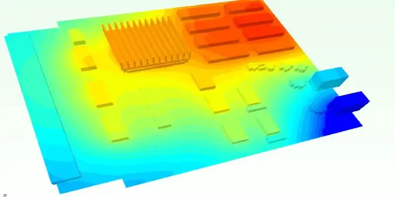
- Use Simulation Tools: Before finalizing your design, use thermal simulation software to model heat flow and identify optimal via placement. This can save time and prevent costly redesigns.
- Work with Your Manufacturer: Collaborate closely with your PCB fabrication partner to ensure they can support copper-filled vias or other thermal management features within your budget.
- Test Under Real Conditions: After prototyping, test your PCB under actual operating conditions, such as high ambient temperatures or full power loads, to verify thermal performance.
- Iterate Based on Data: Measure junction temperatures using thermal cameras or sensors during testing. Use this data to refine via placement or add complementary cooling solutions.
Conclusion: Mastering Thermal Management for LEDs with Thermal Vias
Thermal vias are a game-changer in LED PCB design, offering a compact and efficient way to manage heat in high-power LED applications. By reducing junction temperatures, they boost LED efficiency, extend lifespan, and ensure reliable performance even in demanding environments. When combined with other LED cooling techniques like metal core PCBs and heat sinks, thermal vias provide a robust solution for thermal management for LEDs.
Designing with thermal vias requires careful planning—from via placement and size to material selection and integration with other cooling methods. By following the best practices outlined in this guide, you can create high-power LED PCBs that stay cool under pressure and deliver outstanding results for your lighting projects.


