 ALLPCB


Designing breakaway tabs for SMT stencils is a critical step in ensuring efficient and accurate PCB assembly. These small features allow for easy separation of individual boards from a larger panel after the soldering process, without damaging the components or the board itself. In this comprehensive guide, we’ll walk you through the process of designing effective breakaway tabs for SMT (Surface Mount Technology) stencils, while also covering essential topics like smt stencils pcb, pcb stencils, solder paste application tips, reflow soldering tips, and stencil design best practices. Whether you’re a seasoned engineer or just starting with PCB design, this blog will provide actionable insights to improve your workflow.
What Are Breakaway Tabs and Why Are They Important for SMT Stencils?
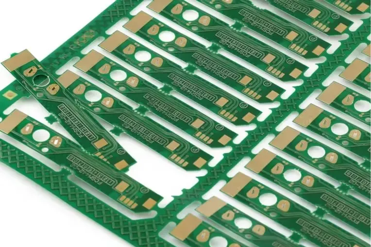
Breakaway tabs, also known as mouse bites or perforated tabs, are small, strategically placed connectors that hold multiple PCBs together in a panel during manufacturing. These tabs are designed to be strong enough to keep the panel intact during processes like solder paste application and reflow soldering, but weak enough to be easily broken apart by hand or with minimal force after assembly.
For smt stencils pcb applications, breakaway tabs are essential because they enable efficient handling of multiple boards at once, reducing production time and costs. Without well-designed tabs, you risk damaging delicate components or the board edges during separation. Properly designed tabs ensure clean breaks, minimal stress on the PCB, and a smoother manufacturing process.
Key Considerations Before Designing Breakaway Tabs
Before diving into the design process, it’s important to understand the factors that influence the effectiveness of breakaway tabs in pcb stencils. Let’s break down the key considerations:
- Board Material and Thickness: The type of material (e.g., FR4) and the thickness of the PCB (e.g., 1.6mm or 0.8mm) affect how much force is needed to break the tabs. Thicker boards may require larger or fewer tabs to ensure stability.
- Component Placement: Components near the edges of the board can be at risk during separation. Tabs should be placed away from sensitive areas to avoid mechanical stress.
- Manufacturing Equipment: Ensure that your panel design, including tab placement, is compatible with the pick-and-place machines and reflow ovens used in production.
- Panel Size: Larger panels may need more tabs for stability, while smaller panels can often use fewer tabs with simpler designs.
Step-by-Step Guide to Designing Breakaway Tabs for SMT Stencils
Now that we’ve covered the basics, let’s dive into a detailed, step-by-step process for designing breakaway tabs tailored for smt stencils pcb workflows. Follow these steps to ensure precision and reliability in your designs.
Step 1: Plan Tab Placement
The first step is to decide where to place the breakaway tabs on your PCB panel. Ideally, tabs should be positioned along the edges of individual boards, away from critical components or traces. A common practice is to place tabs at the corners or midpoints of each board edge. For a standard 100mm x 100mm board, placing two tabs per edge (total of 8 tabs per board) often provides a good balance of stability and ease of separation.
Ensure that the tabs are evenly spaced to distribute stress uniformly during handling. Avoid placing tabs too close to vias or delicate surface-mount components, as the breaking process could cause micro-cracks or damage.
Step 2: Determine Tab Dimensions
The size and shape of the tabs are crucial for their functionality. A typical breakaway tab consists of a narrow bridge of material with small holes (often called mouse bites) drilled along the break line to weaken it. Standard dimensions for tabs are:
- Tab Width: 3-5mm for most PCBs with a thickness of 1.6mm.
- Hole Diameter: 0.8-1.2mm, spaced 1-2mm apart.
- Number of Holes: 3-5 holes per tab, depending on the board thickness and material strength.
These dimensions can be adjusted based on your specific board requirements. For thinner boards (e.g., 0.8mm), reduce the tab width to 2-3mm to make separation easier.
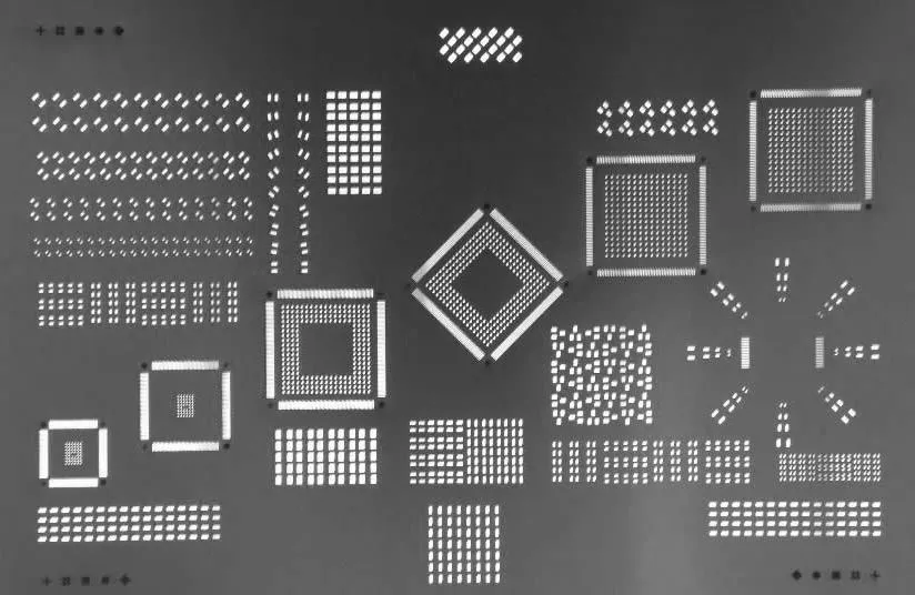
Step 3: Design the Mouse Bites
Mouse bites are the small perforations that make the tabs easy to break. Use your PCB design software to create a series of evenly spaced holes along the tab. Most software tools allow you to define a drill pattern for this purpose. Ensure the holes are aligned precisely along the separation line to avoid jagged edges after breaking.
Step 4: Test the Design
Before finalizing your design, create a prototype panel and test the breakaway tabs. Check if the tabs hold the panel together during handling and if they break cleanly without excessive force. If the tabs are too strong, increase the number or size of the holes. If they’re too weak, reduce the perforations or increase the tab width.
Step 5: Integrate with Stencil Design
When designing breakaway tabs, consider how they align with your SMT stencil. The stencil, used for solder paste application tips, must account for the panel layout. Ensure that the stencil apertures (openings for solder paste) are not obstructed by the tab areas. Additionally, confirm that the stencil material (usually stainless steel, 0.1-0.15mm thick) can withstand the panel handling process without warping.
Stencil Design Best Practices for SMT Assembly
While designing breakaway tabs, it’s also important to follow stencil design best practices to ensure a seamless SMT process. A well-designed stencil directly impacts the quality of solder paste application and, ultimately, the reliability of the soldered joints. Here are some key tips:
- Aperture Size: Match the stencil aperture size to the PCB pad size. For most surface-mount components, a 1:1 ratio works well, but for fine-pitch components (e.g., 0.5mm pitch), reduce the aperture by 10-20% to prevent excess paste.
- Stencil Thickness: Use a stencil thickness of 0.1mm for fine-pitch components and 0.15mm for larger components to control the volume of solder paste deposited.
- Material Quality: Opt for laser-cut stainless steel stencils for precision and durability, especially for high-volume production.
- Cleaning: Regularly clean the stencil to avoid paste buildup, which can lead to uneven application. Use isopropyl alcohol and a lint-free cloth for best results.
Solder Paste Application Tips for Optimal Results
Effective solder paste application tips are vital when working with pcb stencils. The goal is to deposit the right amount of paste onto the PCB pads for reliable soldering. Follow these guidelines to improve your process:
- Use the Right Squeegee: A metal squeegee with a 60-degree angle provides consistent pressure and even paste distribution across the stencil.
- Control Pressure and Speed: Apply moderate pressure (around 2-3 kg) and maintain a slow, steady speed (20-30mm/s) when moving the squeegee to avoid defects like bridging or insufficient paste.
- Inspect After Printing: Use a magnifying glass or automated optical inspection (AOI) to check for issues like misalignment or excess paste before moving to reflow soldering.
- Store Paste Properly: Keep solder paste refrigerated (2-10°C) when not in use to maintain its viscosity and prevent drying out.
Reflow Soldering Tips for SMT Assembly
After applying solder paste, the next step is reflow soldering, where the paste melts to form solid joints between components and pads. Here are some reflow soldering tips to ensure success:
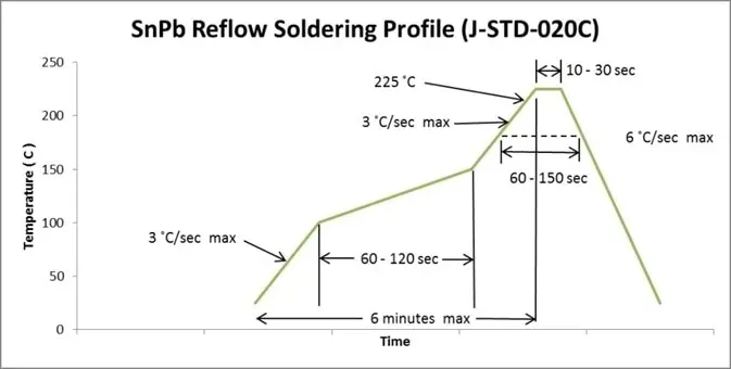
- Temperature Profile: Follow the recommended reflow profile for your solder paste (typically provided by the manufacturer). A common profile includes a preheat stage (150-180°C for 60-90 seconds), a soak stage (180-200°C for 60 seconds), and a reflow stage (peak at 235-245°C for 20-40 seconds).
- Even Heating: Ensure your reflow oven provides uniform heat distribution to avoid cold spots that can lead to incomplete soldering.
- Avoid Thermal Shock: Gradually ramp up and cool down the temperature to prevent thermal stress on components and the PCB.
- Ventilation: Use proper ventilation or a fume extractor to remove harmful fluxes released during reflow.
Common Mistakes to Avoid When Designing Breakaway Tabs and Stencils
Even with careful planning, mistakes can happen. Here are some common pitfalls to watch out for when designing breakaway tabs and working with smt stencils pcb:
- Overloading Tabs: Too many or overly thick tabs can make separation difficult, risking damage to the board. Stick to the recommended dimensions and spacing.
- Poor Tab Placement: Tabs placed too close to components can cause mechanical stress during separation, leading to cracked solder joints or broken parts.
- Inconsistent Stencil Apertures: Incorrect aperture sizes or misalignment in the stencil can result in uneven solder paste application, leading to defects like bridging or tombstoning.
- Ignoring Panel Stability: Insufficient tabs or weak designs can cause the panel to flex during handling, misaligning components or causing paste smearing.
Conclusion: Mastering Breakaway Tabs and SMT Stencil Design
Designing breakaway tabs for SMT stencils is a small but crucial aspect of PCB assembly that can significantly impact production efficiency and product quality. By carefully planning tab placement, sizing, and perforations, you can ensure clean separation without damaging your boards. Additionally, adhering to stencil design best practices, following solder paste application tips, and implementing effective reflow soldering tips will further enhance your SMT process.
Whether you’re working on a small prototype or high-volume production, these guidelines will help you create reliable pcb stencils and panels tailored to your needs. With attention to detail and a focus on precision, you can streamline your workflow and achieve consistent, high-quality results in every project.


