 ALLPCB


If you're looking to optimize your PCB production process, a PCB panel size calculator is an essential tool to maximize board yield and minimize waste. By calculating the ideal panel size and layout for your printed circuit boards (PCBs), you can fit more boards on a single panel, reduce material costs, and streamline manufacturing. In this comprehensive guide, we'll explore how to calculate PCB panel size, the benefits of PCB panelization software, and the best practices for using PCB panel optimization tools to achieve the highest yield per panel.
What Is a PCB Panel Size Calculator and Why Does It Matter?
A PCB panel size calculator is a tool or PCB design software that helps designers and manufacturers determine the most efficient way to arrange multiple PCB designs on a single panel. Panels are large sheets of material used during manufacturing to produce several boards at once. The goal is to fit as many boards as possible onto a panel while minimizing wasted space and ensuring the layout meets manufacturing constraints like spacing for routing and tooling holes.
Using a calculator or optimization tool is critical because inefficient panel layouts can lead to higher costs and longer production times. For instance, if only 60% of a panel is used for actual boards, the remaining 40% is wasted material, driving up expenses. With the right tools, you can increase panel utilization to 85% or more, saving money and resources.
Understanding PCB Panelization: The Basics
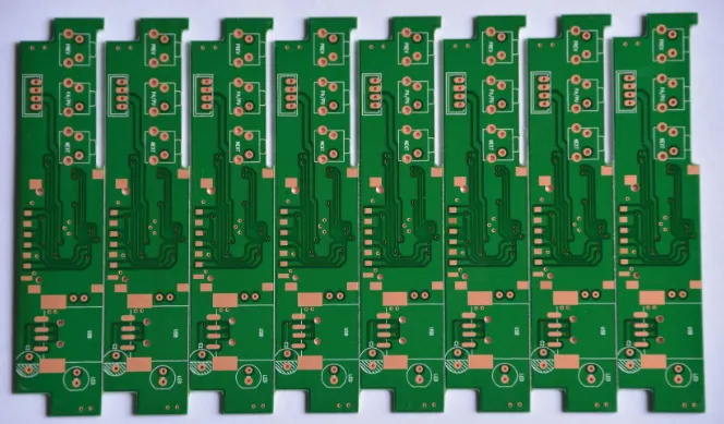
Before diving into calculators and software, let’s cover the basics of PCB panelization. Panelization is the process of grouping multiple PCB designs (or copies of the same design) onto a single panel for manufacturing. This approach reduces handling time, simplifies assembly, and lowers costs by producing many boards in one go.
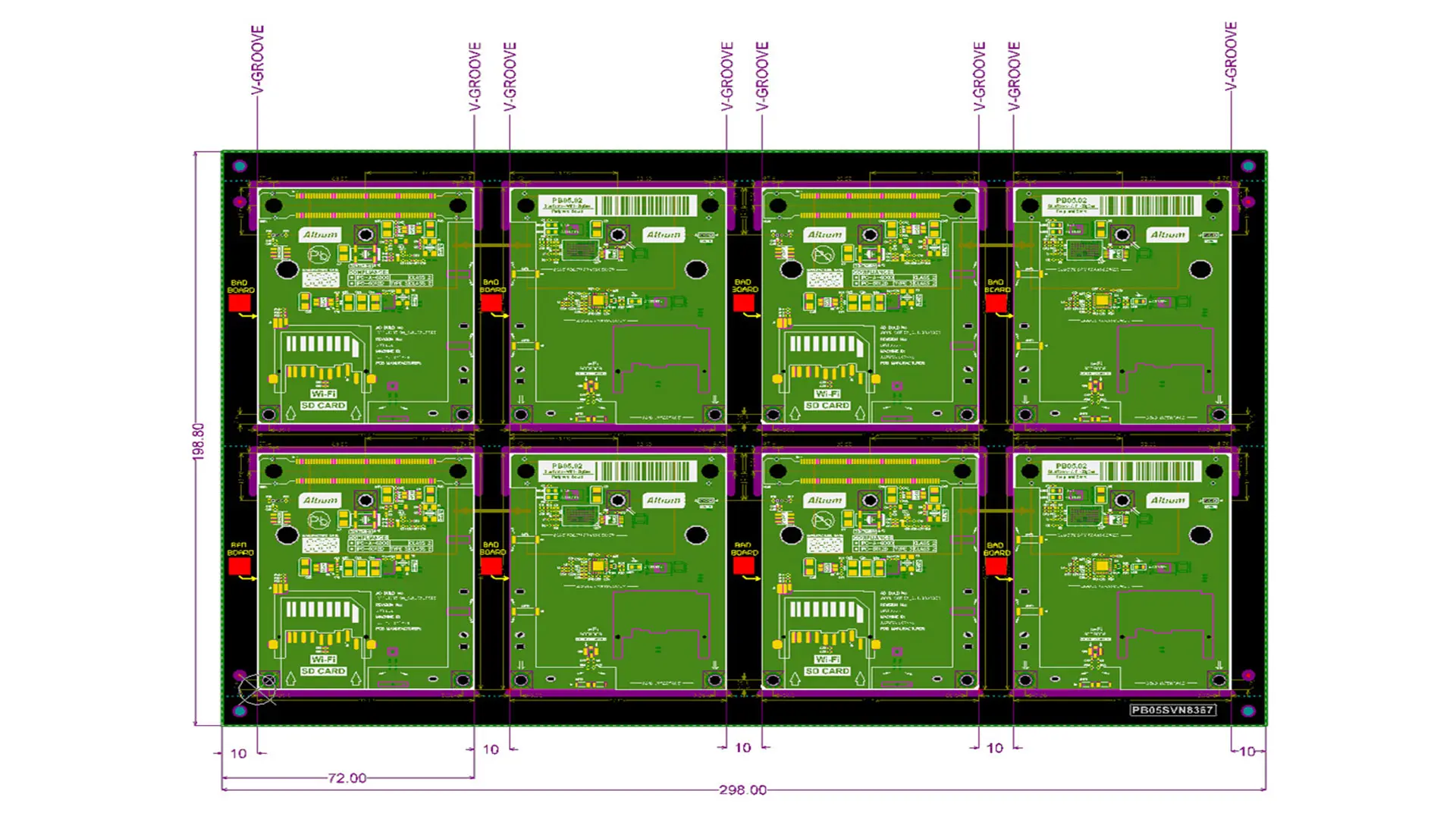
However, panelization isn’t just about placing boards randomly. Factors like board size, shape, spacing for cutting (usually 2-3 mm between boards), and panel edge clearance (often 10 mm) must be considered. A well-panelized design ensures that boards can be easily separated after production without damage, while also maximizing the number of boards per panel.
How to Calculate PCB Panel Size Manually
Calculating PCB panel size manually is a good starting point for understanding the process, though it can be time-consuming for complex designs. Here’s a step-by-step guide to help you get started:
- Determine Your Board Dimensions: Measure the length and width of your individual PCB design. For example, let’s say your board is 50 mm x 30 mm.
- Account for Spacing: Add spacing between boards for cutting or routing. A common spacing is 2.5 mm on each side. So, your effective board size with spacing becomes 55 mm x 35 mm.
- Know Your Panel Size: Standard panel sizes vary by manufacturer, but common dimensions are 18 inches x 24 inches (457 mm x 610 mm). Check with your production house for exact sizes.
- Calculate Fit: Divide the panel dimensions by your effective board size to see how many boards fit along each axis. For a 457 mm x 610 mm panel, you could fit approximately 8 boards along the width (457 / 55 = 8.3, rounded down to 8) and 17 along the length (610 / 35 = 17.4, rounded down to 17). This gives you 136 boards per panel (8 x 17).
- Adjust for Edge Clearance: Subtract edge clearance (e.g., 10 mm on each side) from the panel dimensions before calculating. With clearance, the usable area might be 437 mm x 590 mm, reducing the fit to 7 boards along the width and 16 along the length, or 112 boards total.
While manual calculations work for simple designs, they don’t account for irregular shapes, rotation of boards for better fit, or other manufacturing constraints. This is where PCB panel calculators and software come into play.
The Power of PCB Panel Calculators for Optimization
A PCB panel calculator automates the process of determining how many boards can fit on a panel, saving time and reducing errors. These tools often allow you to input your board dimensions, desired spacing, and panel size to instantly get a layout suggestion. Some calculators even provide a visual representation of the panel, showing exactly how the boards will be arranged.
For example, if you’re working with a board size of 75 mm x 50 mm and a panel size of 400 mm x 500 mm, a calculator can quickly tell you that rotating the boards 90 degrees might increase the yield from 20 boards to 24 per panel. This kind of insight is invaluable for minimizing waste and maximizing efficiency.
Many online tools are free and easy to use, making them accessible even for small-scale designers or hobbyists. By inputting a few key numbers, you can experiment with different layouts to find the most cost-effective solution.
Suggested Reading:Standard PCB Panel Sizes: Optimizing Your Layout for Efficient Manufacturing
Advanced PCB Panelization Software for Maximum Yield
While basic calculators are great for simple projects, PCB panelization software takes optimization to the next level. These programs are designed for professional engineers and manufacturers who need to handle complex designs, multiple board types, or high-volume production runs. Here are some key features of advanced software:
- Automatic Nesting: The software arranges boards in the most efficient way possible, often rotating or flipping them to fit more units on a panel. This can increase yield by 10-15% compared to manual layouts.
- Multi-Design Support: If you’re producing different board designs on the same panel, the software can mix and match them to minimize empty space.
- Constraint Management: It accounts for manufacturing rules like minimum spacing, edge clearance, and tooling requirements, ensuring the panel is production-ready.
- Cost Estimation: Some tools calculate material usage and provide cost estimates based on the panel layout, helping you make budget-friendly decisions.
Using such software, a PCB manufacturer might increase panel utilization from 70% to 90%, significantly reducing material waste. For a production run of 10,000 boards, even a 5% improvement in yield can save hundreds of dollars in raw materials.
Benefits of Maximizing PCB Yield Per Panel
Maximizing PCB yield per panel offers several advantages that directly impact your bottom line and production efficiency. Let’s break down the key benefits:
1. Cost Reduction
More boards per panel mean less material waste and lower per-unit costs. If a panel costs $50 to produce and you fit 100 boards instead of 80, your cost per board drops from $0.63 to $0.50—a 20% savings.
2. Faster Production
Producing more boards in a single run reduces the number of panels needed, speeding up manufacturing. This is especially important for high-volume orders where time is critical.
3. Environmental Impact
Minimizing waste reduces the amount of unused PCB material (like fiberglass and copper) that ends up in landfills. Efficient panelization is a small but meaningful step toward sustainable manufacturing.
4. Improved Quality Control
Panelized boards are often processed together, ensuring consistent quality across a batch. Fewer panels also mean less handling, reducing the risk of damage during production.
Best Practices for PCB Panel Optimization
To get the most out of PCB panel calculators and optimization tools, follow these best practices during the design and manufacturing stages:
- Design with Panelization in Mind: Keep board dimensions as uniform as possible to simplify layout. Avoid overly complex shapes unless necessary, as they can reduce nesting efficiency.
- Communicate with Your Manufacturer: Different production houses have unique panel sizes and spacing requirements. Share your design early to ensure compatibility with their processes.
- Use Breakaway Tabs or V-Grooves: These methods make it easier to separate boards after production without wasting space. Tabs typically require 5-8 mm of space, while V-grooves need even less.
- Test Different Orientations: Sometimes rotating a board 90 or 180 degrees can dramatically improve fit. Many tools allow you to experiment with orientations for the best results.
- Account for Tooling Holes: Reserve space for tooling holes or fiducials (usually 3-5 mm in diameter) needed for alignment during assembly. Place them in areas that don’t interfere with board placement.
Common Challenges in PCB Panelization and How to Overcome Them
Even with the best tools, panelization can present challenges. Here are a few common issues and solutions:
Irregular Board Shapes
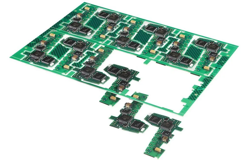
Non-rectangular boards can leave gaps on a panel, reducing yield. Use software with advanced nesting algorithms to fit irregular shapes together like puzzle pieces, or consider redesigning the board for a more panel-friendly shape if possible.
Overcrowding
Packing too many boards too closely can lead to cutting errors or damage during separation. Always adhere to minimum spacing guidelines (typically 2-3 mm) to avoid issues.
Panel Size Limitations
If your manufacturer uses smaller panels than expected, your calculated layout might not work. Double-check panel dimensions upfront and design with flexibility in mind to accommodate different sizes.
Choosing the Right PCB Panel Optimization Tools
With so many PCB panel calculators and software options available, selecting the right one depends on your needs. Here are some factors to consider:
- Ease of Use: For beginners or small projects, look for simple online calculators with intuitive interfaces.
- Features: For professional use, choose software with advanced features like automatic nesting, multi-design support, and manufacturing rule checks.
- Integration: Some tools integrate with PCB design software, allowing you to export designs directly into a panel layout.
- Cost: While many basic calculators are free, advanced software might require a subscription or one-time purchase. Weigh the custom PCB cost against the potential savings from optimized yields.
Conclusion: Optimize Your PCB Production with Panel Calculators
Maximizing board yield and minimizing waste is a critical aspect of efficient PCB manufacturing, and a PCB panel size calculator is your best ally in achieving this goal. Whether you’re manually calculating layouts or using advanced PCB panelization software, the right approach can save you time, reduce costs, and improve the sustainability of your production process. By following best practices and leveraging PCB panel optimization tools, you can ensure that every inch of material is used effectively, delivering high-quality boards at a lower cost.
Start exploring different tools today to find the one that fits your workflow. With the right strategy, you’ll see significant improvements in your PCB yield per panel, making your manufacturing process smoother and more profitable.


