 ALLPCB


Are you looking to streamline your PCB manufacturing process and reduce costs? Understanding standard PCB panel sizes and optimizing your layout through effective panelization is the key to achieving efficient production. In this comprehensive guide, we’ll dive into the PCB panelization process, explore standard PCB panel dimensions benefits, and share actionable tips on PCB depaneling methods, PCB routing techniques, and improving PCB manufacturing yield. Whether you're a design engineer or a manufacturer, this post will help you maximize efficiency and quality in your projects.
What Are Standard PCB Panel Sizes and Why Do They Matter?
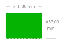
Standard PCB panel sizes refer to the commonly used dimensions of larger boards on which multiple smaller PCBs are arranged during manufacturing. These panels are designed to fit the equipment and processes used in fabrication and assembly, ensuring compatibility and cost-effectiveness. Common panel sizes include 18 x 24 inches (457 x 610 mm), 21 x 24 inches (533 x 610 mm), and 18 x 21 inches (457 x 533 mm), though these can vary based on the manufacturer’s capabilities and regional standards.
Using standard panel sizes matters because it directly impacts production efficiency. When your PCB design aligns with these dimensions, you minimize material waste, reduce setup times, and lower costs. Non-standard sizes often lead to higher expenses due to custom tooling or inefficient use of panel space. By optimizing your layout for standard sizes, you can achieve a higher PCB manufacturing yield and streamline the entire production process.
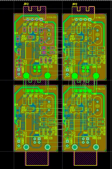
Understanding the PCB Panelization Process
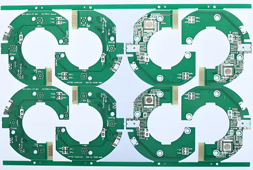
The PCB panelization process involves arranging multiple individual PCB designs onto a single larger panel for manufacturing. This technique is essential for mass production as it allows manufacturers to process several boards at once, saving time and reducing handling costs. Let’s break down the key steps in this process:
- Design Layout: Engineers arrange individual PCB designs on the panel, ensuring proper spacing for cutting and handling. Typically, a gap of 2-3 mm between boards is recommended to allow for depaneling tools.
- Adding Breakaway Tabs or V-Grooves: These features are included to facilitate the separation of individual boards after assembly. Tabs are small connections holding the boards together, while V-grooves are scored lines for easier cutting.
- Tooling Holes and Fiducials: Tooling holes (usually 3-4 per panel) are added for alignment during manufacturing, while fiducial markers help automated assembly machines locate the board accurately.
- Panel Border: A border of 5-10 mm around the panel edge is often left clear for handling and to accommodate manufacturing equipment clamps.
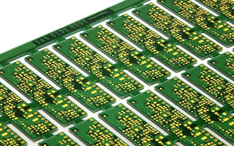
Effective panelization reduces material waste and ensures smoother production runs. For example, fitting 20 small PCBs (each 50 x 50 mm) on an 18 x 24-inch panel with minimal wasted space can cut costs by up to 30% compared to producing each board individually.
Benefits of Standard PCB Panel Dimensions
Aligning your designs with standard PCB panel dimensions benefits both the manufacturer and the designer in several ways. Here’s why it’s a smart choice:
- Cost Reduction: Standard sizes match the capabilities of most manufacturing equipment, avoiding the need for custom setups that drive up costs. For instance, using an 18 x 24-inch panel can save up to 15-20% on material costs compared to non-standard dimensions.
- Faster Turnaround: Since standard panels are compatible with automated machinery, production times are shorter. This can reduce lead times by 1-2 days on average.
- Higher Yield: Optimized layouts on standard panels mean more boards per panel, improving PCB manufacturing yield. A well-designed panel might yield 50 boards instead of 40, directly impacting profitability.
- Reduced Waste: Standard sizes maximize panel usage, leaving less scrap material. This not only cuts costs but also supports sustainable manufacturing practices.
By focusing on these dimensions, you ensure a smoother workflow from design to delivery, saving both time and money.
Optimizing Layout with PCB Routing Techniques
PCB routing techniques play a critical role in optimizing panel layouts for efficient manufacturing. Routing refers to the process of creating paths for electrical signals on the board, but in the context of panelization, it also involves planning the physical separation of boards. Here are some proven techniques to consider:
- Tab Routing: This method uses small tabs to hold individual PCBs together on the panel. The tabs are designed with perforations or mouse bites (small drill holes) to make separation easier. Typically, 3-5 tabs per board, spaced evenly, provide stability without complicating depaneling.
- V-Scoring: V-scoring involves creating shallow grooves along the separation lines of the panel. These grooves weaken the material, allowing boards to be snapped apart manually or with minimal force. A standard V-score depth is about 30-40% of the board thickness (e.g., 0.6 mm for a 1.6 mm thick board).
- Panel Edge Clearance: Ensure a clearance of at least 5 mm from the panel edge to avoid damage during handling. This also provides space for routing tools and prevents stress on components near the edge.
- Component Placement: Avoid placing components too close to the board edges (maintain a 2-3 mm setback) to prevent damage during routing or depaneling processes.
Using these techniques, you can create a panel layout that balances manufacturing ease with board integrity. For example, combining tab routing with V-scoring on a panel of 30 small boards can reduce depaneling time by 50% compared to using tabs alone.
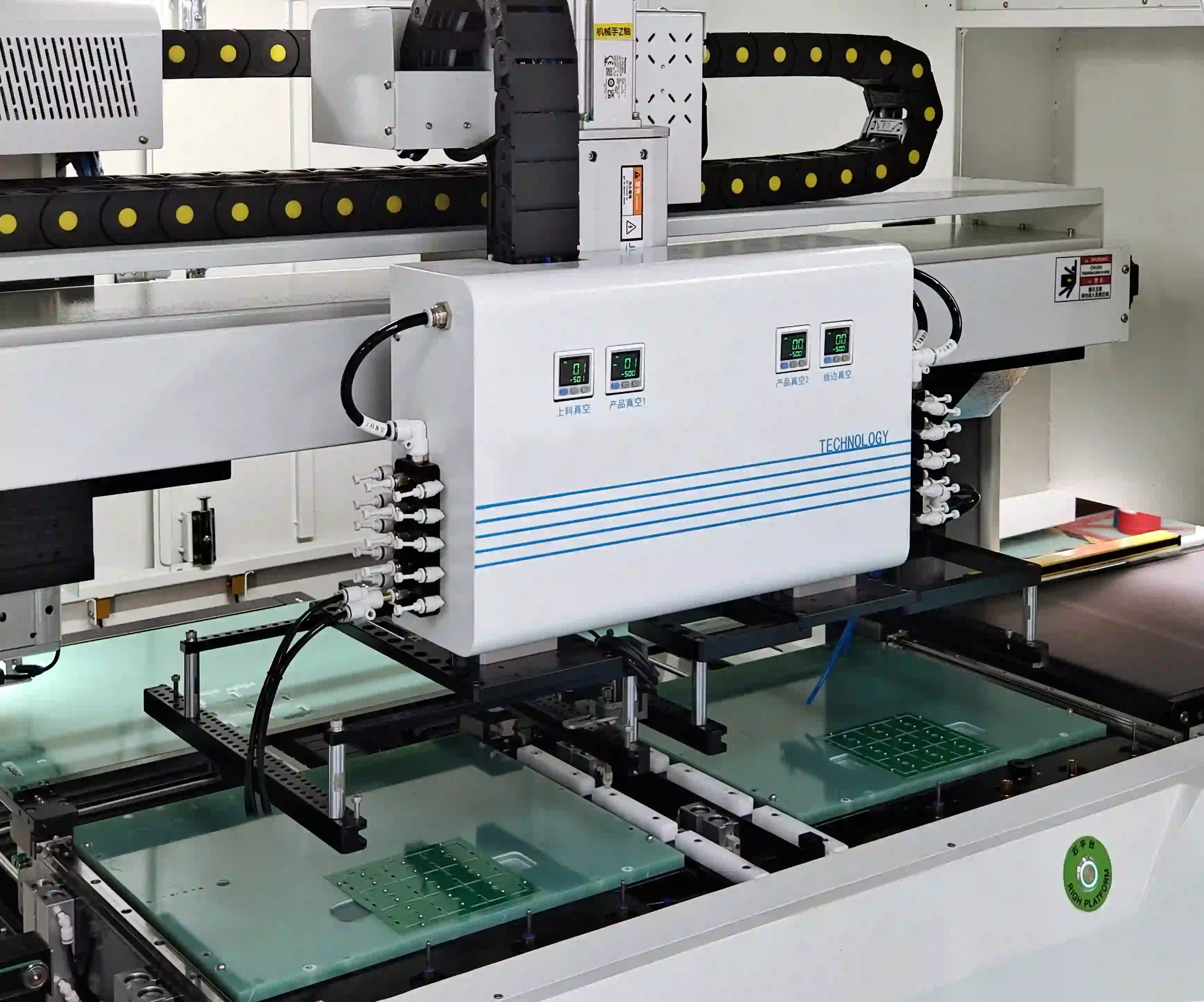
PCB Depaneling Methods: Separating Boards with Precision
After manufacturing, individual PCBs need to be separated from the panel—a process known as depaneling. Choosing the right PCB depaneling methods ensures that boards are separated without damaging components or traces. Here are the most common methods:
- Manual Breakaway: For panels with breakaway tabs or V-grooves, boards can often be separated by hand. This method is cost-effective for low-volume production but risks stress on components if not done carefully.
- Pizza Cutter Tool: This handheld tool uses a rotating blade to cut along V-grooves, offering more precision than manual breaking. It’s ideal for medium-volume runs and reduces the risk of board damage.
- Router Depaneling: For high precision, a CNC router cuts along predefined paths to separate boards. This method is best for complex designs or when tabs are used, as it minimizes stress. However, it’s slower and more expensive, often costing 20-30% more than manual methods.
- Laser Depaneling: Using a laser to cut boards provides the highest precision and is ideal for delicate or high-density designs. It’s the most expensive option, with costs potentially 50% higher than routing, but it eliminates mechanical stress entirely.
The choice of depaneling method depends on your production volume, board complexity, and budget. For instance, a small run of 100 simple boards might use manual breakaway to save costs, while a run of 10,000 high-density boards could justify the investment in laser depaneling for quality assurance.
Maximizing PCB Manufacturing Yield Through Panelization
Improving PCB manufacturing yield—the number of usable boards produced per panel—is a primary goal of effective panelization. A higher yield means lower costs per board and better overall profitability. Here are some strategies to maximize yield:
- Efficient Nesting: Arrange boards on the panel to minimize unused space. Software tools can help optimize nesting, often increasing yield by 10-15%. For example, rotating boards by 90 degrees might allow you to fit 25 boards instead of 20 on a panel.
- Consistent Board Sizes: If possible, design boards with uniform dimensions for a given project. This simplifies panelization and reduces wasted space. Mixing different sizes often leads to a 5-10% drop in yield due to inefficient spacing.
- Minimize Tooling Area: Reduce the number of tooling holes or fiducials to only what’s necessary (e.g., 3 holes instead of 5) to free up space for additional boards.
- Test Panels Early: Before full production, create a test panel to identify layout issues. Fixing problems early can prevent a 20-30% yield loss due to design errors.
By focusing on these strategies, you can significantly boost the number of usable boards per panel, directly impacting your bottom line. A well-optimized panel for a 50 x 50 mm board might yield 48 units instead of 40, a 20% improvement.
Practical Tips for Designing Panels for Efficient Manufacturing
To wrap up, here are some actionable tips to ensure your panel designs lead to efficient manufacturing:
- Consult with Manufacturers Early: Share your design files during the planning stage to confirm panel size compatibility and get feedback on layout optimization.
- Use Design Software: Leverage PCB design tools with panelization features to automate layout and spacing, reducing errors and saving time.
- Balance Cost and Quality: While maximizing board count per panel is important, don’t compromise on spacing or depaneling features that protect board integrity.
- Account for Material Thickness: Standard PCB thicknesses like 1.6 mm work best with most depaneling methods. Thicker boards (e.g., 2.4 mm) may require deeper V-scores or stronger tools, increasing costs by 10-15%.
Conclusion: Streamline Your PCB Production with Optimized Panelization
Mastering standard PCB panel sizes and the PCB panelization process is a game-changer for efficient manufacturing. By aligning your designs with standard dimensions, using effective PCB routing techniques, and selecting the right PCB depaneling methods, you can significantly boost PCB manufacturing yield and cut costs. The standard PCB panel dimensions benefits are clear: reduced waste, faster production, and higher profitability.
Start by reviewing your current layouts and identifying opportunities to optimize panel usage. With the tips and strategies shared in this guide, you’re well-equipped to take your PCB production to the next level. Focus on precision in design and collaboration with your manufacturing partner to ensure every panel delivers maximum value.


