 ALLPCB


When it comes to separating individual printed circuit boards (PCBs) from a larger panel during manufacturing, choosing the right depaneling method is critical for efficiency, cost, and board integrity. Two popular techniques, V-scoring (also known as V-cut) and stamp hole depaneling, offer distinct advantages depending on your project needs. So, which method should you choose? In short, V-scoring is ideal for straight-line separations and high-volume production due to its clean cuts and low stress on components, while stamp hole depaneling suits smaller batches or irregular board shapes with its flexibility and minimal tooling costs. This blog dives deep into the details of both methods, covering PCB V-scoring advantages and disadvantages, the stamp hole depaneling process, V-cut design guidelines, stamp hole design specifications, and tips for depaneling method selection to help you make an informed decision.
What is PCB Depaneling and Why Does It Matter?
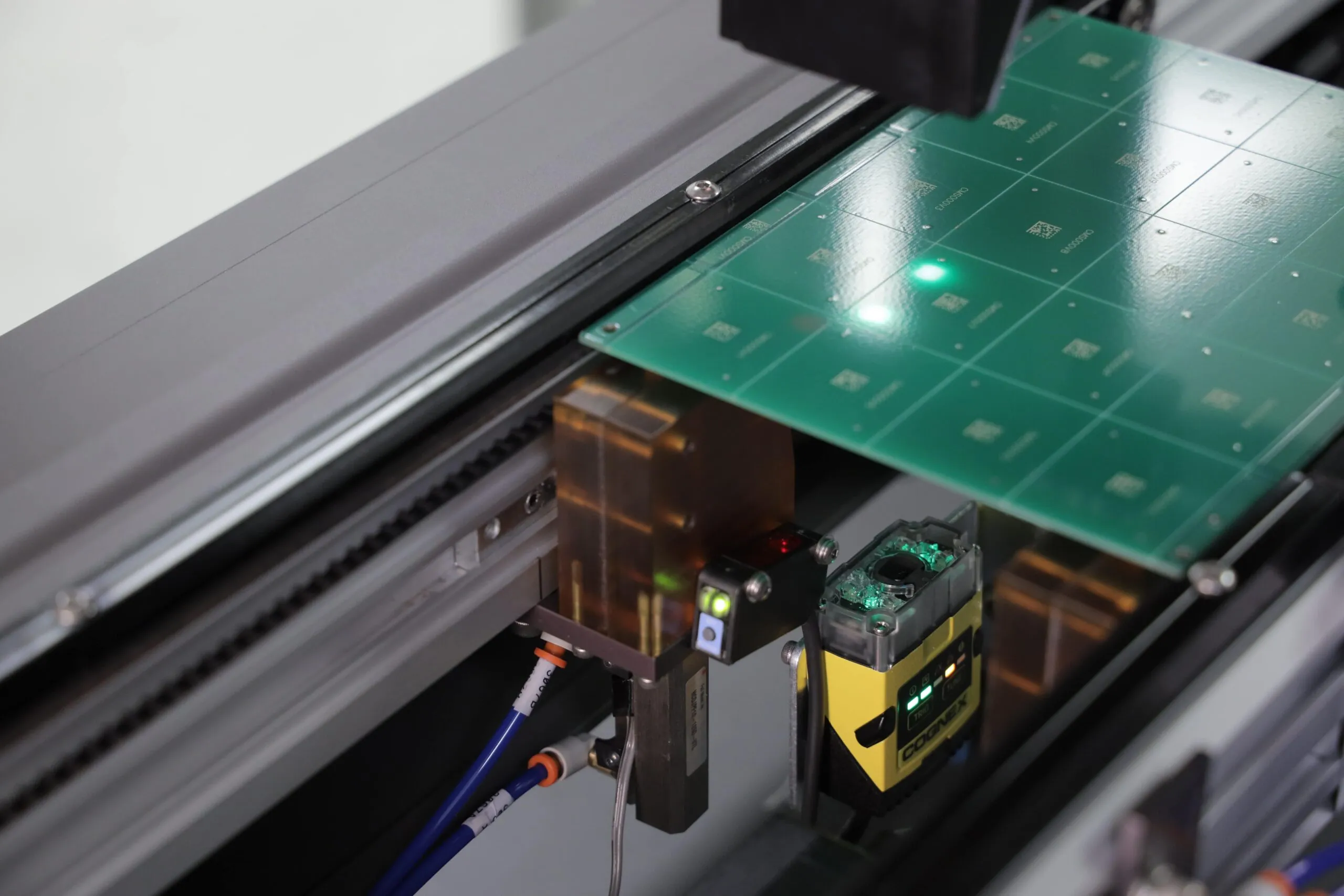
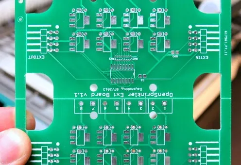
PCB depaneling is the process of separating individual circuit boards from a larger panel after fabrication. Manufacturers often produce multiple PCBs on a single panel to save time and reduce costs during assembly. However, separating these boards without damaging components, traces, or the board itself is a delicate task. The depaneling method you choose impacts not only the quality of the final product but also production speed, cost, and scalability.
Selecting the wrong method can lead to issues like cracked solder joints, damaged edges, or increased manufacturing expenses. That’s why understanding the differences between V-scoring and stamp hole depaneling is essential for engineers and manufacturers aiming for optimal results.
Understanding V-Scoring (V-Cut) Depaneling
V-scoring, often referred to as V-cut, involves creating a V-shaped groove on both sides of the PCB panel using a specialized cutting tool. This groove weakens the material along a straight line, making it easy to snap the boards apart manually or with minimal force. V-scoring is widely used in high-volume PCB production due to its precision and efficiency.
PCB V-Scoring Advantages
- Clean and Precise Separation: The V-cut creates a smooth edge with minimal burrs, reducing the need for additional finishing. This is ideal for boards where aesthetics or edge quality matter.
- Low Stress on Components: Since the separation requires minimal force, there’s less risk of damaging nearby components or solder joints. Studies show that V-scoring can reduce mechanical stress by up to 60% compared to other manual methods.
- Cost-Effective for High Volumes: V-scoring machines can process large panels quickly, making it economical for mass production runs of 10,000 units or more.
- Suitable for Automated Assembly: The consistent grooves allow for automated depaneling equipment, further speeding up production.
PCB V-Scoring Disadvantages
- Limited to Straight Lines: V-scoring only works for straight separations. If your PCB design has curved or irregular shapes, this method won’t work.
- Not Ideal for Thick Boards: V-cuts are less effective on boards thicker than 3.2 mm, as the groove may not penetrate deeply enough for easy separation.
- Component Placement Restrictions: Components cannot be placed too close to the V-cut line (typically within 0.5 mm), as the cutting process can cause vibration or stress.
V-Cut Design Guidelines
To ensure successful V-scoring, follow these design tips:
- Groove Depth: The V-cut should penetrate about one-third of the board thickness on each side. For a 1.6 mm thick board, aim for a 0.5 mm deep groove per side, leaving a 0.6 mm web of material to break.
- Minimum Board Spacing: Keep at least 0.3 mm of spacing between individual boards to allow for the V-cut tool’s width.
- Component Clearance: Maintain a clearance of at least 0.5 mm between components and the V-cut line to avoid damage during cutting or separation.
- Board Thickness: V-scoring works best on boards between 0.6 mm and 3.2 mm thick. Thicker boards may require alternative methods.
- Material Compatibility: Ensure your PCB material (e.g., FR-4) is suitable for V-scoring, as some flexible or brittle materials may crack unpredictably.
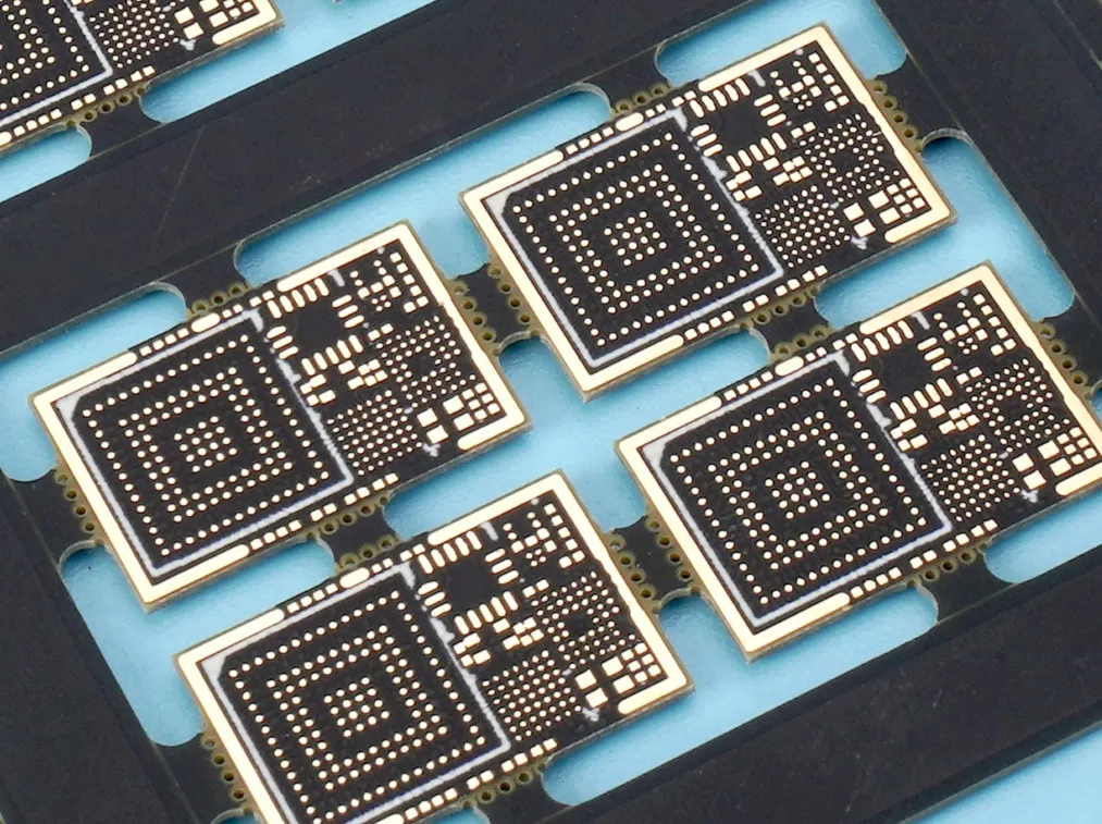
Understanding Stamp Hole Depaneling
Stamp hole depaneling, also known as mouse bites, involves drilling a series of small holes along the edges where individual PCBs connect to the panel or to each other. These holes weaken the connection, allowing the boards to be snapped apart by hand. This method is often used for smaller production runs or when V-scoring isn’t feasible.
Stamp Hole Depaneling Process
The stamp hole process is straightforward:
- Design: During PCB layout, small holes (typically 0.8 mm to 1.2 mm in diameter) are placed along the separation line, spaced closely together (often 0.2 mm to 0.5 mm apart).
- Drilling: These holes are drilled into the panel during fabrication, creating a perforated line similar to the edge of a postage stamp.
- Separation: After PCB assembly, the individual boards are snapped apart manually by breaking the thin strips of material between the holes.
Stamp Hole Design Specifications
For effective stamp hole depaneling, adhere to these specifications:
- Hole Diameter: Use holes between 0.8 mm and 1.2 mm in diameter. Smaller holes may not weaken the material enough, while larger holes can waste board space.
- Hole Spacing: Space holes 0.2 mm to 0.5 mm apart to ensure easy separation without compromising panel stability during assembly.
- Number of Holes: For a 10 mm separation line, 5 to 8 holes are typically sufficient, depending on material thickness and strength.
- Edge Clearance: Keep components at least 1 mm away from the stamp hole line to prevent damage during snapping.
- Material Thickness: Stamp holes work well on boards up to 2.0 mm thick. Thicker boards may require more force to separate, risking damage.
Advantages of Stamp Hole Depaneling
- Flexibility in Design: Unlike V-scoring, stamp holes can be used for irregular or curved separation lines, making them versatile for unique board shapes.
- Low Tooling Costs: Stamp holes don’t require specialized cutting tools beyond standard drilling equipment, reducing setup costs for small runs (under 1,000 units).
- Suitable for Small Batches: This method is ideal for prototyping or low-volume production where investing in V-scoring equipment isn’t justified.
Disadvantages of Stamp Hole Depaneling
- Rough Edges: The snapping process often leaves rough or jagged edges, which may require additional sanding or finishing for aesthetic or functional purposes.
- Higher Stress on Boards: Breaking the boards apart can create more mechanical stress, risking damage to nearby components or traces. Stress levels can be up to 40% higher compared to V-scoring.
- Not Ideal for High Volumes: Manual separation is time-consuming, making stamp holes less efficient for large production runs of 5,000 units or more.
Comparing V-Scoring and Stamp Hole Depaneling: Key Differences
To help with depaneling method selection, let’s compare these two techniques across critical factors:
| Factor | V-Scoring (V-Cut) | Stamp Hole |
|---|---|---|
| Separation Line | Straight lines only | Straight or irregular lines |
| Edge Quality | Smooth, clean edges | Rough, jagged edges |
| Stress on Components | Low (up to 60% less stress) | Higher (up to 40% more stress) |
| Production Volume | Best for high volumes (10,000+ units) | Best for low volumes (under 1,000 units) |
| Tooling Cost | Higher due to specialized equipment | Lower, uses standard drilling |
| Board Thickness | 0.6 mm to 3.2 mm | Up to 2.0 mm |
Depaneling Method Selection: How to Choose the Right One
Choosing between V-scoring and stamp hole depaneling depends on your project’s specific requirements. Consider these factors to guide your decision:
- Production Volume: For large-scale production (over 5,000 units), V-scoring is more efficient and cost-effective due to automation capabilities. For prototypes or small runs (under 1,000 units), stamp holes offer a cheaper and quicker solution.
- Board Design: If your PCB layout requires straight-line separation, V-scoring is the better choice for clean results. For irregular or curved separations, opt for stamp holes.
- Edge Quality Needs: If smooth edges are critical for your application (e.g., for enclosures or customer-facing products), V-scoring delivers superior results. If edge quality isn’t a priority, stamp holes can suffice.
- Component Density: For densely populated boards with components near the edges, V-scoring minimizes stress and damage. Stamp holes may pose a higher risk due to the force needed for separation.
- Budget Constraints: If tooling costs are a concern, stamp holes require less investment upfront since they use standard drilling processes.
- Board Thickness and Material: Check if your board thickness falls within the recommended range for each method. Also, ensure the material (e.g., standard FR-4 vs. flexible substrates) is compatible with the chosen technique.
Suggested Reading: Depaneling Demystified: Choosing the Right Method for Your PCB Panel Size
Best Practices for Implementing Your Chosen Depaneling Method
Once you’ve selected a depaneling method, follow these best practices to ensure success:
- Collaborate Early with Your Manufacturer: Share your design files and discuss depaneling preferences during the initial stages to avoid costly revisions. Specify tolerances and clearances to prevent issues.
- Test with Prototypes: Before full production, create a small batch to test the depaneling process. For V-scoring, check if the groove depth allows easy snapping without excessive force. For stamp holes, verify that the hole spacing ensures clean separation without damaging the board.
- Optimize Component Placement: Keep sensitive components away from separation lines, adhering to the clearance guidelines (0.5 mm for V-cut, 1 mm for stamp holes).
- Document Specifications: Include detailed notes in your design files about the depaneling method, groove depth, or hole spacing to avoid miscommunication during manufacturing.
Common Challenges and How to Avoid Them
Both V-scoring and stamp hole depaneling come with potential pitfalls. Here’s how to address them:
- Cracked Boards During Separation: For V-scoring, ensure the groove depth is consistent across the panel. For stamp holes, avoid spacing holes too far apart, as this increases the force needed to snap the boards.
- Damaged Components: Maintain proper clearance between components and separation lines to reduce vibration or stress impact.
- Inconsistent Edges: With stamp holes, rough edges are common. Plan for post-separation finishing if smooth edges are required. For V-scoring, use high-quality cutting tools to avoid uneven grooves.
Conclusion: Making the Right Choice for Your PCB Project
Deciding between V-scoring and stamp hole depaneling boils down to understanding your project’s unique needs. V-scoring shines in high-volume production with its clean cuts, low stress, and automation compatibility, making it perfect for straight-line separations on standard boards. On the other hand, stamp hole depaneling offers flexibility for irregular shapes and lower costs for small runs, though it sacrifices edge quality and increases mechanical stress.
By considering factors like production volume, board design, edge quality, and budget, you can confidently select the best depaneling method. Use the V-cut design guidelines and stamp hole design specifications provided in this guide to optimize your PCB layout for manufacturing. With careful planning and collaboration with your manufacturing partner, you’ll achieve efficient, damage-free depaneling that meets your project goals.
For more insights into PCB manufacturing processes or to get started on your next project, explore our resources and services tailored to engineers and designers looking for reliable solutions.


