 ALLPCB


In high-speed PCB design, optimizing via-to-via spacing is critical for maintaining signal integrity. Proper spacing minimizes issues like crosstalk, impedance mismatches, and return loss, ensuring reliable performance in modern electronics. This blog dives deep into the importance of via spacing for signal integrity, practical strategies for high-speed PCB design, and techniques for via impedance control, return loss optimization, and crosstalk minimization.
Why Via-to-Via Spacing Matters in High-Speed PCB Design
Vias are essential in printed circuit boards (PCBs) as they connect different layers, allowing signals to travel through the board. However, in high-speed designs where signals operate at gigahertz frequencies, poorly spaced vias can disrupt signal integrity. When vias are too close, they can cause electromagnetic interference, leading to crosstalk and signal degradation. On the other hand, spacing them too far apart may complicate routing and increase board size unnecessarily.
Signal integrity refers to the quality of an electrical signal as it travels through a PCB. Issues like crosstalk, where signals interfere with each other, or return loss, where part of the signal is reflected back due to impedance mismatches, can degrade performance. Optimizing via-to-via spacing helps address these challenges, ensuring signals remain clear and reliable even at high speeds.
Understanding Signal Integrity Challenges in High-Speed PCBs
High-speed PCBs, often used in applications like telecommunications, data centers, and consumer electronics, operate at frequencies where even small design flaws can lead to significant problems. Let’s explore the key challenges related to via spacing and signal integrity issues.
Crosstalk and Electromagnetic Interference
Crosstalk happens when signals from one via or trace interfere with another due to electromagnetic coupling. In high-speed designs, this can distort data and cause errors. Vias placed too close together act like antennas, picking up unwanted signals from nearby vias or traces. Studies show that crosstalk can increase by over 20% when via spacing is reduced below a critical threshold, often around 3 to 5 times the via diameter, depending on the dielectric material and signal frequency.
Impedance Mismatches and Return Loss
Impedance control is crucial for ensuring signals travel without reflection. Vias introduce discontinuities in the signal path, altering the impedance. If vias are not spaced correctly, these discontinuities worsen, leading to higher return loss. For instance, at 5 GHz, a via spacing of less than 0.5 mm in a standard FR-4 material can cause a return loss increase of up to 10 dB, severely impacting signal quality.
Signal Delay and Timing Issues
In high-speed designs, timing is everything. Closely spaced vias can create parasitic capacitance and inductance, slowing down signal propagation. This delay can desynchronize data streams, especially in applications like DDR memory or high-speed serial links operating at 10 Gbps or higher.
Best Practices for Via-to-Via Spacing in High-Speed PCB Design
Now that we understand the challenges, let’s look at actionable strategies to optimize via spacing for enhanced signal integrity. These practices focus on via impedance control, return loss optimization, and crosstalk minimization.
1. Determine Optimal Via Spacing Based on Frequency
The ideal via-to-via spacing depends on the signal frequency. As a rule of thumb, higher frequencies require greater spacing to reduce coupling. For signals above 1 GHz, maintain a spacing of at least 3 to 5 times the via diameter. For example, with a via diameter of 0.2 mm, aim for a spacing of 0.6 to 1.0 mm. At 10 GHz, you might need to increase this to 1.2 mm or more to keep crosstalk below acceptable levels (typically under -30 dB).
2. Use Ground Vias for Shielding
Placing ground vias near signal vias can act as a shield, reducing crosstalk. Ground vias help create a return path for high-speed signals, minimizing electromagnetic interference. A common approach is to surround critical signal vias with ground vias at a distance of about 1.5 to 2 times the signal via diameter. This technique can reduce crosstalk by up to 15-20% in designs operating at 5 GHz or higher.
3. Control Via Impedance with Proper Design
Via impedance control is vital for minimizing return loss. Use simulation tools to model the impedance of vias based on their diameter, length, and spacing. For instance, a via with a diameter of 0.3 mm and a length of 1.6 mm in a 4 layer PCB might have an impedance of around 50 ohms if designed correctly. Adjusting the spacing to avoid clustering helps maintain this impedance, preventing reflections. Keeping return loss below -10 dB often requires fine-tuning via placement during the layout phase.
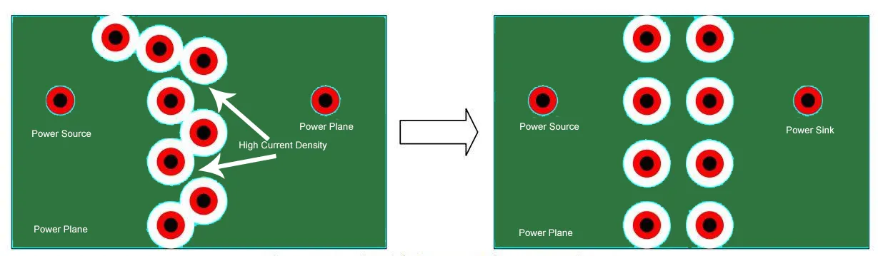
4. Route Traces Away from Via Clusters
Avoid routing high-speed traces near densely packed vias. The electromagnetic fields around vias can couple with traces, causing signal distortion. If routing near vias is unavoidable, ensure a separation of at least 3 trace widths and consider using differential pairs to cancel out interference. This practice is especially important for signals operating at speeds above 2.5 Gbps.
5. Minimize Via Stub Lengths
Via stubs—unused portions of a via that extend beyond the signal path—can act as resonant structures, amplifying noise and return loss at specific frequencies. Use back-drilling to remove stubs or design blind and buried vias for critical high-speed signals. For a 10 GHz signal, a stub length as small as 0.5 mm can cause a noticeable increase in return loss, sometimes exceeding -5 dB.
Advanced Techniques for Crosstalk Minimization and Return Loss Optimization
Beyond basic spacing rules, advanced techniques can further enhance performance in high-speed PCB design. These methods require careful planning and often the use of simulation software.
Differential Pair Via Design
For high-speed serial links, differential pairs are commonly used to transmit data. When designing vias for differential pairs, maintain symmetry in spacing and placement to ensure balanced impedance. A spacing mismatch as small as 0.1 mm between differential vias can introduce skew, degrading signal integrity at speeds above 5 Gbps. Keep the via-to-via spacing within the pair tight (around 1.5 times the via diameter) while spacing the pair away from other signals by at least 3 times that distance.
Simulation and Modeling for Via Spacing
Simulation tools are invaluable for optimizing via spacing. Software can model electromagnetic fields, predict crosstalk levels, and calculate return loss for different via configurations. For example, at 8 GHz, simulations might show that a via spacing of 0.8 mm results in crosstalk of -35 dB, while reducing it to 0.4 mm increases crosstalk to -20 dB. Use these insights to fine-tune your design before manufacturing.
Layer Stackup Optimization
The PCB layer stackup affects how vias interact with signals. Place high-speed signals on layers with continuous ground planes to provide a stable return path. Avoid placing vias near the edge of ground planes, as this can disrupt the return current and increase return loss. A well-designed 6-layer stackup with dedicated ground and power planes can reduce crosstalk by up to 10% compared to a poorly planned layout.
Material Selection for High-Speed PCB Performance
The choice of PCB material also influences via spacing and signal integrity. Standard FR-4 material, with a dielectric constant (Dk) of around 4.2, works for frequencies up to about 1 GHz. For higher frequencies, consider low-loss materials with a Dk of 3.0 or below. These materials reduce signal delay and crosstalk, allowing for tighter via spacing without sacrificing performance. For instance, using a material with a Dk of 3.0 can reduce crosstalk by approximately 8-12% compared to FR-4 at 5 GHz.
Practical Tips for Implementing Via Spacing in Your Designs
Here are some final tips to ensure your via spacing strategy succeeds in high-speed PCB design:
- Start with design guidelines based on signal speed and adjust based on simulation results.
- Collaborate with your PCB manufacturer to understand fabrication limits for via sizes and spacing.
- Test prototypes under real-world conditions to validate signal integrity before full production.
- Document via spacing rules in your design library for consistency across projects.
Conclusion: Achieving Signal Integrity Through Via Spacing
Optimizing via-to-via spacing is a cornerstone of high-speed PCB design. By addressing challenges like crosstalk, impedance mismatches, and return loss, you can ensure reliable performance in demanding applications. Focus on practical spacing rules, use ground vias for shielding, and leverage simulation tools for precise via impedance control and crosstalk minimization. With these strategies, your designs will meet the stringent requirements of modern electronics, delivering clear signals at even the highest speeds.
Whether you’re working on data communication systems or cutting-edge consumer devices, proper via spacing for signal integrity is a skill worth mastering. Apply these principles in your next project to see measurable improvements in performance and reliability.


