 ALLPCB


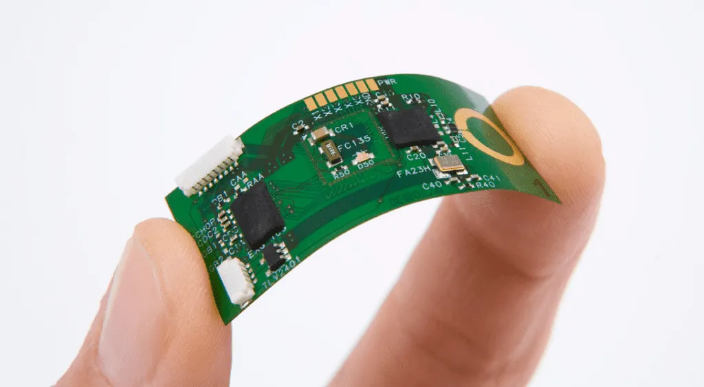
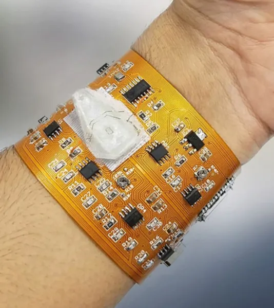
Flexible printed circuit boards (PCBs) are essential in modern electronics, enabling compact, lightweight, and versatile designs for devices like wearables, medical equipment, and automotive systems. However, imaging for flexible circuits poses unique challenges due to their thin, bendable materials and intricate designs. In this blog post, we’ll explore the key hurdles in flexible PCB imaging, such as material sensitivity and precision requirements, and provide practical solutions like Laser Direct Imaging (LDI) and high-resolution techniques to overcome them. Whether you're navigating flex circuit manufacturing or seeking to improve imaging accuracy, this guide offers actionable insights to help you succeed.
Introduction to Flexible PCB Imaging
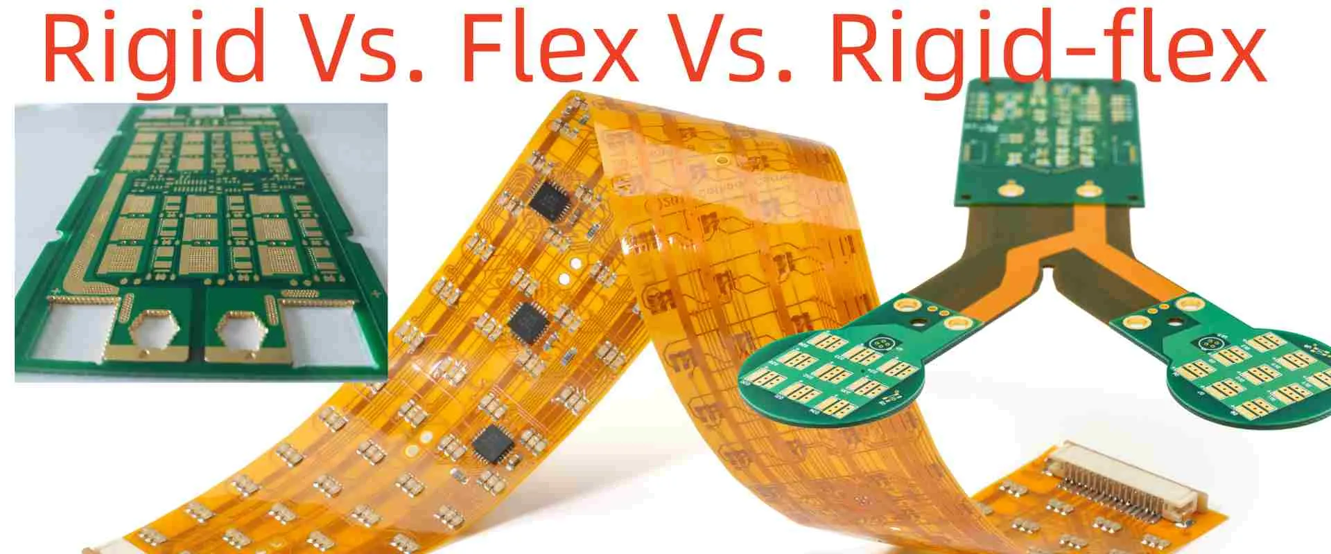
Flexible PCBs, often called flex circuits, are designed to bend and conform to unique shapes, making them ideal for space-constrained applications. Imaging, a critical step in PCB manufacturing, involves transferring circuit patterns onto the substrate using techniques like photolithography or direct imaging. For flexible circuits, this process is far from straightforward. The materials used, such as polyimide, are sensitive to heat and mechanical stress, while the need for high-resolution patterns demands cutting-edge technology.
In this comprehensive guide, we’ll dive into the specific challenges of imaging for flexible PCBs and highlight innovative solutions that ensure precision and reliability. From traditional methods to advanced LDI for flexible PCBs, we’ll cover everything you need to know to optimize your flex circuit manufacturing process.
What Makes Flexible PCB Imaging So Challenging?
Imaging flexible circuits is inherently more complex than working with rigid PCBs due to several factors. Let’s break down the primary challenges that manufacturers face when dealing with flex circuits.
1. Material Sensitivity and Flexibility
Flexible PCBs are typically made from materials like polyimide or polyester, which are thinner and more delicate than the FR-4 used in rigid boards. These materials can deform, stretch, or tear under mechanical stress during imaging. Additionally, they are sensitive to temperature and chemical exposure, which can cause dimensional changes or damage during processes like photolithography. For instance, a temperature increase of just 10°C can lead to a dimensional shift of up to 0.02% in polyimide, affecting alignment accuracy.
2. High-Resolution Requirements
Modern flex circuits often require extremely fine traces and tight tolerances to accommodate compact designs. Achieving line widths as narrow as 25 micrometers (μm) or smaller is common in high-resolution flex PCBs, especially for applications like wearable sensors. Traditional imaging methods struggle to maintain such precision over flexible substrates, leading to defects like line breaks or short circuits.
3. Registration and Alignment Issues
Due to the flexible nature of the substrate, maintaining precise registration during imaging is a significant hurdle. Even slight misalignments can result in pattern distortions, impacting the functionality of the circuit. This challenge is amplified in multilayer flex designs, where multiple layers must align perfectly. A misalignment of just 10 μm can cause signal integrity issues, especially in high-frequency applications where impedance control is critical (e.g., maintaining 50 ohms for RF signals).
4. Handling Thin and Lightweight Materials
Flexible substrates are often less than 50 μm thick, making them prone to wrinkling or buckling during handling. This can lead to uneven exposure during imaging, resulting in incomplete or blurry patterns. Manufacturers must use specialized equipment and processes to ensure the material remains flat and stable throughout the imaging stage.
Solutions for Imaging Challenges in Flexible PCBs
Despite these challenges, advancements in technology and manufacturing techniques have paved the way for effective solutions. Below, we explore proven methods to address the hurdles of flexible PCB imaging, ensuring high precision and reliability in flex circuit manufacturing.
1. Laser Direct Imaging (LDI) for Flexible PCBs
Laser Direct Imaging (LDI) has emerged as a game-changer for imaging flexible circuits. Unlike traditional photolithography, which relies on masks and film, LDI uses a laser to directly write circuit patterns onto the photoresist-coated substrate. This method offers several advantages for flex circuits:
- Enhanced Precision: LDI can achieve resolutions as fine as 15 μm, making it ideal for high-resolution flex PCBs. This level of accuracy ensures clear, sharp traces even on delicate materials.
- Better Registration: Since LDI eliminates the need for physical masks, it reduces alignment errors. Digital data drives the laser, ensuring consistent pattern placement across the substrate.
- Material Compatibility: LDI operates without excessive heat or mechanical stress, minimizing the risk of dimensional changes in sensitive materials like polyimide.
For example, in applications requiring high-frequency signal transmission, such as 5G devices, LDI can maintain tight impedance control by ensuring trace widths and spacing remain within tolerances of ±5 μm.
2. Advanced Photoresist Materials
Choosing the right photoresist is critical for successful imaging on flexible substrates. Modern photoresists are formulated to adhere better to flexible materials and withstand the stresses of bending and processing. Liquid photoresists, for instance, can conform to the surface irregularities of thin substrates, ensuring uniform coating and exposure. These materials also offer improved resolution, supporting line widths below 20 μm for intricate designs.
3. Specialized Handling Equipment
To address the issue of handling thin, lightweight materials, manufacturers can use vacuum tables or automated roll-to-roll systems. These tools keep the substrate flat and stable during imaging, preventing wrinkles or distortions. Roll-to-roll processing, in particular, is ideal for high-volume production of flexible circuits, as it minimizes manual handling and ensures consistent tension across the material.
4. High-Resolution Imaging Techniques
Beyond LDI, other high-resolution imaging techniques, such as inkjet printing with conductive inks, are gaining traction in flex circuit manufacturing. These additive methods deposit conductive material directly onto the substrate, eliminating the need for etching and reducing material waste. While still emerging, this approach shows promise for achieving resolutions below 30 μm, especially for ultra-thin flexible circuits used in medical implants.
Best Practices for Optimizing Flexible PCB Imaging
To achieve the best results in flexible PCB imaging, manufacturers should adopt a combination of advanced technologies and process optimizations. Here are some actionable best practices to consider:
- Invest in LDI Technology: For projects requiring high-resolution flex PCBs, LDI is a worthwhile investment. Its ability to handle fine features and multilayer designs makes it a must-have for cutting-edge applications.
- Control Environmental Factors: Maintain stable temperature and humidity levels in the manufacturing environment to prevent dimensional changes in flexible substrates. For instance, keeping the workspace at 22°C ± 2°C can minimize material expansion or contraction.
- Use Simulation Software: Before imaging, use design simulation tools to predict potential alignment issues or signal integrity problems. This step can save time and reduce costly errors during production.
- Test and Iterate: Conduct small-scale pilot runs to test imaging parameters on specific flexible materials. Adjust exposure times, laser power, or photoresist thickness based on the results to achieve optimal outcomes.
Applications of High-Resolution Flex PCBs
The advancements in imaging techniques for flexible circuits have opened doors to a wide range of applications. High-resolution flex PCBs are now integral to industries where precision and compactness are paramount. Some notable examples include:
- Wearable Technology: Devices like smartwatches and fitness trackers rely on flex circuits with fine traces to fit complex electronics into small, curved spaces.
- Medical Devices: Flexible PCBs are used in implantable devices and diagnostic tools, where high-resolution imaging ensures reliable performance in critical applications.
- Automotive Systems: Flex circuits in sensors and control units must withstand vibration and temperature fluctuations, making precise imaging essential for durability.
Future Trends in Flexible PCB Imaging
The field of flexible PCB imaging is evolving rapidly, driven by the demand for smaller, more powerful electronics. Emerging trends include the integration of artificial intelligence (AI) to optimize imaging parameters in real-time, further improving precision and reducing defects. Additionally, additive manufacturing techniques, such as 3D printing of conductive materials, are being explored to create fully customized flex circuits with unprecedented design freedom.
Another exciting development is the use of environmentally friendly materials and processes in flex circuit manufacturing. Green fabrication methods aim to reduce chemical waste during imaging and etching, aligning with global sustainability goals while maintaining high performance.
Conclusion
Imaging for flexible PCBs presents unique challenges, from material sensitivity to the need for high-resolution patterns. However, with innovative solutions like Laser Direct Imaging (LDI) for flexible PCBs, advanced photoresists, and specialized handling equipment, manufacturers can overcome these hurdles and achieve exceptional results. By adopting best practices and staying ahead of emerging trends, you can ensure precision and reliability in flex circuit manufacturing, no matter the complexity of your project.


