 ALLPCB


In the fast-evolving world of artificial intelligence, AI accelerator PCBs are at the heart of high-performance computing. These specialized circuit boards demand robust power delivery networks (PDN) to ensure stable operation under intense workloads. If you're an engineer or designer working on AI hardware, optimizing power integrity is critical to achieving efficiency and reliability. This guide dives deep into the essentials of PDN design for AI accelerators, covering key aspects like voltage regulator placement, decoupling capacitors, and power plane impedance.
Whether you're tackling issues with AI accelerator PCB power integrity or seeking best practices for PDN design for AI, this comprehensive resource will walk you through actionable strategies and technical insights to enhance your designs. Let's explore how to build a solid foundation for power delivery in AI accelerator PCBs.
Why Power Delivery Networks Matter for AI Accelerator PCBs
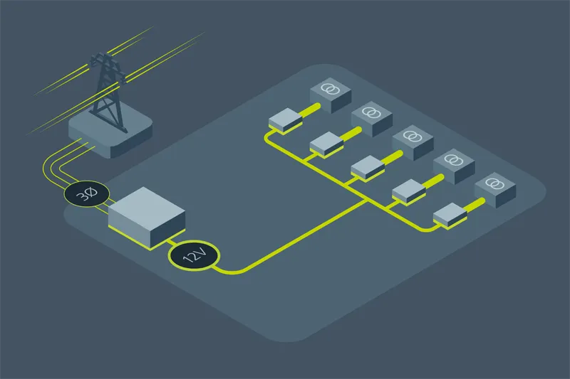
AI accelerators, such as GPUs and TPUs, handle massive data processing tasks that require significant power. These chips often operate at low voltages (e.g., 0.8V to 1.2V) with high current demands, sometimes exceeding 100A. Any fluctuation or noise in the power supply can lead to performance drops, data errors, or even hardware failure. A well-designed power delivery network ensures stable voltage levels, minimizes noise, and supports the high-speed switching of modern AI chips.
The stakes are high with AI accelerator PCB power integrity. Poor PDN design can result in voltage droops during sudden load changes, electromagnetic interference (EMI), and overheating. By focusing on PDN optimization, you can improve system reliability and extend the lifespan of your hardware. Let’s break down the critical components of PDN design for AI accelerators.
Key Elements of PDN Design for AI Accelerator PCBs
Designing an effective PDN for AI hardware involves balancing several factors, including voltage regulation, current distribution, and noise suppression. Below, we’ll cover the core elements that directly impact AI accelerator performance.
1. Voltage Regulator Placement on AI PCBs
Voltage regulator placement on AI PCBs is a foundational step in PDN design. Voltage regulators convert input power to the precise low voltages required by AI chips. Placing them close to the load (the AI accelerator) minimizes voltage drops caused by trace resistance and inductance. For example, a trace with a resistance of just 1 mΩ can cause a 100 mV drop at 100A, which is significant for a chip operating at 1V.
To optimize placement, position voltage regulators as near as possible to the power pins of the AI chip. This reduces the length of high-current paths and lowers parasitic inductance. Additionally, ensure that the input and output capacitors for the regulator are placed nearby to stabilize the voltage. Many designs use point-of-load (POL) regulators directly on the PCB to achieve this proximity.
Another tip is to distribute multiple regulators around larger AI chips with high power demands. This approach, often called "multi-phase regulation," balances current delivery and reduces thermal stress on individual components. Proper voltage regulator placement on AI PCBs is a critical factor in maintaining power integrity.

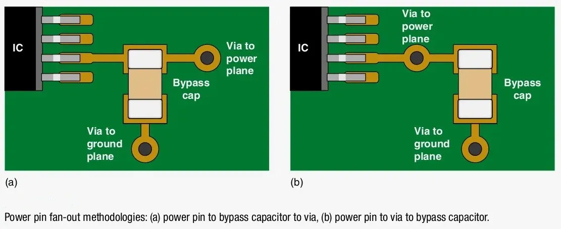
2. Role of Decoupling Capacitors in AI Accelerators
Decoupling capacitors are essential for maintaining AI accelerator PCB power integrity. These components act as local energy reservoirs, supplying instantaneous current during rapid load changes. AI accelerators frequently switch between low and high power states, creating transient current demands that can cause voltage spikes or droops if not addressed.
For effective decoupling in AI accelerators, use a combination of capacitors with different values (e.g., 0.1 μF, 1 μF, and 10 μF) placed at various distances from the chip. Smaller capacitors with low equivalent series inductance (ESL) should be closest to the power pins to handle high-frequency noise, while larger bulk capacitors can be slightly farther away to manage lower-frequency fluctuations.
A common guideline is to place at least one small decoupling capacitor (e.g., 0.1 μF) within 1-2 mm of each power pin on the AI chip. This minimizes inductance in the power delivery path, ensuring a clean supply. Additionally, spread decoupling capacitors evenly across the board to avoid localized voltage drops. By optimizing the use of decoupling capacitors in AI accelerators, you can significantly reduce noise and improve performance.
3. Managing Power Plane Impedance on AI PCBs
Power plane impedance on AI PCBs is another critical aspect of PDN design. Power planes are large copper layers in the PCB stack-up that distribute power across the board. Their impedance, which includes resistance and inductance, directly affects how efficiently power reaches the AI chip. High impedance can lead to voltage drops and noise, especially at high frequencies.
To minimize power plane impedance, use thick copper layers (e.g., 2 oz or higher) for power and ground planes. Thicker copper reduces resistance, allowing for better current flow. Additionally, keep power and ground planes closely spaced in the PCB stack-up to lower inductance. A typical spacing of 2-4 mils between planes can achieve a low impedance path for high-frequency currents.
Another strategy is to create dedicated power islands for critical components like the AI accelerator. These isolated regions on the power plane reduce interference from other parts of the circuit. Finally, use multiple vias to connect power planes to the chip’s power pins, as this further lowers impedance by providing parallel current paths. Managing power plane impedance on AI PCBs is vital for maintaining a stable and noise-free power supply.
Best Practices for PDN Design in AI Accelerators
With the core elements covered, let’s explore some best practices for PDN design in AI accelerators. These tips can help you avoid common pitfalls and achieve optimal performance.
Simulate Your PDN Early in the Design Process
Before finalizing your PCB layout, use simulation tools to analyze your PDN. These tools can model voltage drops, current distribution, and impedance across frequencies. For instance, target an impedance of less than 1 mΩ up to 100 MHz for high-performance AI chips to ensure minimal noise. Simulations help identify weak points in your design, such as insufficient decoupling or high-impedance paths, allowing you to make adjustments early.
Balance Thermal and Electrical Performance
AI accelerators generate significant heat, which can affect PDN components like voltage regulators and capacitors. Place heat sinks or thermal vias near high-power areas to dissipate heat effectively. Additionally, choose components with high temperature ratings (e.g., capacitors rated for 105°C or higher) to ensure reliability under thermal stress.
Minimize Loop Inductance in Power Paths
Loop inductance occurs when current travels through long traces or loops between power and ground. High inductance increases impedance and delays current delivery during transients. To minimize this, keep power and return paths as short and direct as possible. Use adjacent power and ground planes to create a low-inductance return path for high-frequency currents.
Prioritize Ground Plane Integrity
A solid, unbroken ground plane is crucial for PDN design in AI accelerators. Avoid splitting the ground plane unless absolutely necessary, as splits can create high-impedance return paths and increase EMI. If splits are unavoidable, use stitching capacitors or vias to bridge the gap and maintain a low-impedance connection.
Common Challenges in AI Accelerator PDN Design and How to Overcome Them
Designing a PDN for AI accelerators comes with unique challenges. Below, we address some common issues and offer solutions to ensure robust power integrity.
High Current Density and Voltage Drops
AI chips often draw currents exceeding 100A, creating high current density in small areas. This can lead to significant voltage drops across traces and planes. To mitigate this, use wider traces (e.g., 50-100 mils for high-current paths) and multiple parallel vias to distribute current evenly. Additionally, consider using bus bars or embedded power planes for extremely high currents.
Noise and EMI from High-Speed Switching
The rapid switching of AI accelerators generates high-frequency noise and EMI, which can interfere with nearby circuits. To reduce noise, place decoupling capacitors strategically as discussed earlier. Also, use shielding techniques, such as enclosing sensitive areas with ground vias, to contain EMI within the PCB.
Space Constraints on Compact PCBs
AI accelerator PCBs are often densely packed, leaving limited space for PDN components. In such cases, prioritize vertical power delivery by stacking regulators and capacitors on both sides of the board. You can also use smaller, high-density components like chip-scale package regulators to save space without compromising performance.
Future Trends in PDN Design for AI Hardware
As AI technology advances, so do the demands on PDN design. Emerging trends include the adoption of vertical power delivery, where power is supplied directly through the chip package or substrate, reducing parasitic effects. Innovations in materials, such as low-loss dielectrics and high-conductivity copper, are also helping to lower impedance and improve efficiency.
Additionally, AI-driven design tools are becoming more prevalent, automating tasks like component placement and impedance optimization. These tools can analyze thousands of layout scenarios in minutes, helping engineers create more efficient PDNs. Staying updated on these trends can give you a competitive edge in designing next-generation AI accelerator PCBs.
Conclusion: Building Reliable Power Delivery for AI Accelerators
Optimizing power delivery networks for AI accelerator PCBs is a complex but essential task. By focusing on key areas like voltage regulator placement, decoupling capacitors, and power plane impedance, you can ensure stable power integrity and maximize the performance of your AI hardware. Implementing best practices, such as early PDN simulation and thermal management, further enhances reliability and efficiency.
Whether you're refining PDN design for AI or addressing specific challenges like high current density, the strategies outlined in this guide provide a solid roadmap. With careful planning and attention to detail, you can build AI accelerator PCBs that meet the rigorous demands of modern computing. Start applying these principles to your next project and see the difference a well-designed PDN can make.


