When it comes to designing printed circuit boards (PCBs) for surface mount technology (SMT), one of the critical decisions is choosing the right minimum drill size for SMT pads. This choice directly impacts solder joint reliability, which is essential for the performance and longevity of electronic devices. In this comprehensive guide, we’ll dive into how to select the optimal drill size for SMT pads, explore its effects on solder paste application and reflow soldering, and provide actionable PCB pad design guidelines to ensure robust solder joints.
Whether you’re an electronics engineer or a PCB designer, understanding the relationship between drill size, pad design, and soldering processes can prevent costly failures and improve manufacturing outcomes. Let’s break down the key factors and best practices to optimize your designs for reliability.
Why Minimum Drill Size Matters for SMT Pads
The drill size used for vias or mounting holes near SMT pads plays a significant role in the overall integrity of the PCB. While SMT components are soldered directly onto the surface of the board, the presence of vias or through-holes in or near pads can affect solder distribution, thermal management, and mechanical stability during reflow soldering. A drill size that’s too large or too small can lead to issues like insufficient solder coverage, weak joints, or even pad lifting during assembly.
For SMT designs, the focus is often on vias-in-pad or nearby vias that connect layers of the PCB. Choosing the right minimum drill size ensures proper solder paste application and prevents defects like solder wicking or voiding. A well-selected drill size also supports the structural integrity of the pad, reducing the risk of cracking or delamination under thermal or mechanical stress.
Key Impacts of Drill Size on Solder Joint Reliability
- Solder Paste Distribution: The size of vias or holes near SMT pads can influence how solder paste spreads during application. Larger holes may cause solder to wick away from the pad, leading to insufficient material for a strong joint.
- Thermal Dissipation: During reflow soldering, drill holes affect heat distribution. Incorrect sizes can cause uneven heating, resulting in poor solder wetting or cold joints.
- Mechanical Strength: Smaller drill sizes can maintain pad integrity, while oversized holes may weaken the pad structure, increasing the risk of cracks or pad cratering.

Understanding PCB Drill Size for SMT Pads
The minimum drill size for vias or holes near SMT pads typically ranges from 0.2 mm to 0.5 mm, depending on the design requirements and manufacturing capabilities. This size refers to the diameter of the drilled hole before plating, which will slightly reduce the final inner diameter. For SMT designs, smaller drill sizes are often preferred to minimize interference with solder paste application and to maintain pad strength.
However, the choice of drill size must balance several factors:
- Aspect Ratio: The ratio of the hole depth to its diameter. A high aspect ratio (deeper hole relative to diameter) can make plating difficult and affect signal integrity. A common guideline is to keep the aspect ratio below 10:1 for reliable manufacturing.
- Pad Size: The SMT pad must be large enough to accommodate the component lead or termination while leaving room for any nearby vias. For example, a 0603 resistor pad might measure 0.8 mm x 0.6 mm, requiring careful placement of any via with a drill size of 0.3 mm.
- Manufacturing Limits: Most PCB fabrication houses can reliably drill holes as small as 0.2 mm, but smaller sizes may increase costs or risk drill bit breakage.
By adhering to these constraints, designers can select a drill size that supports both manufacturability and solder joint reliability.
Optimizing SMT Stencil Design for Solder Paste Application
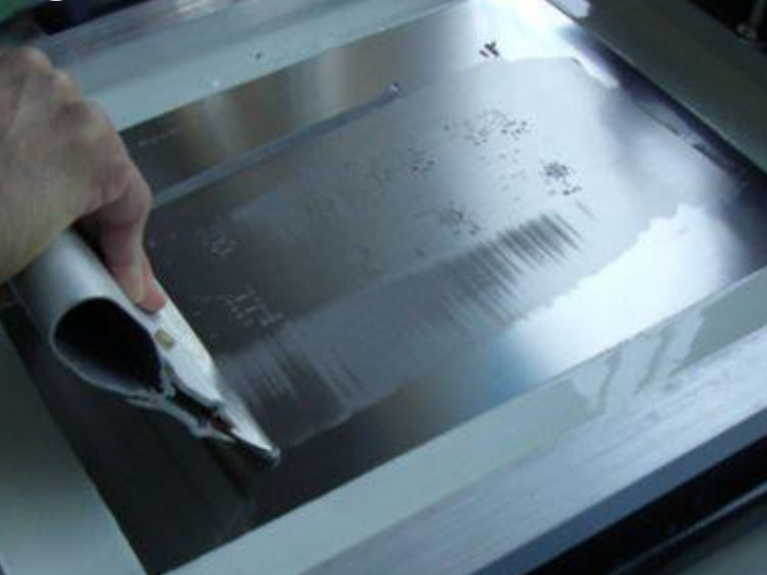
The stencil design is a critical part of the SMT assembly process, as it controls the amount and placement of solder paste on the pads. When vias or holes are present near SMT pads, the stencil design must account for the minimum drill size to prevent solder paste from escaping into the holes during application.
Best Practices for SMT Stencil Design
- Aperture Size: The stencil aperture should match the pad size, typically covering 80-90% of the pad area to avoid excess paste. For pads near vias, reduce the aperture slightly on the side closest to the hole to prevent solder migration.
- Stencil Thickness: A thickness of 0.1 mm to 0.15 mm is common for fine-pitch SMT components. Thicker stencils may deposit too much paste, increasing the risk of bridging, especially near small drill holes.
- Via Tenting: If possible, tent or plug vias near SMT pads to block solder paste from flowing into them. This is especially important for vias with drill sizes larger than 0.3 mm.
Proper stencil design ensures that the solder paste stays on the pad, creating a uniform layer for reflow soldering. This step is vital for achieving consistent and reliable solder joints.

The Role of Reflow Soldering in Solder Joint Reliability
Reflow soldering is the process of melting solder paste to form a permanent bond between the SMT component and the PCB pad. The presence of vias or holes near pads, influenced by the minimum drill size, can impact how heat is distributed and how solder flows during this process.
Key Considerations for Reflow Soldering
- Temperature Profile: Ensure the reflow oven reaches a peak temperature of around 240-260°C for lead-free solder (e.g., SAC305 alloy). Uneven heat distribution caused by large drill holes can lead to cold solder joints or incomplete wetting.
- Solder Wicking: Small drill sizes (e.g., 0.2-0.3 mm) reduce the risk of solder wicking into vias, ensuring enough solder remains on the pad for a strong joint.
- Thermal Mass: Larger vias or holes can act as heat sinks, pulling heat away from the pad. This can be mitigated by using smaller drill sizes or adding thermal relief patterns around vias.
By carefully managing the reflow process and accounting for drill size effects, designers can minimize defects like voiding or tombstoning, where components lift off one side of the pad.
PCB Pad Design Guidelines for SMT Reliability
Designing SMT pads with the right dimensions and configurations is essential for achieving reliable solder joints. Here are detailed guidelines to follow, tailored to account for minimum drill sizes and their impact on assembly.
1. Pad Sizing for SMT Components
Pad sizes should match the component footprint as recommended by the manufacturer or industry standards like IPC-7351. For example:
- 0402 Resistor/Capacitor: Pad size of 0.5 mm x 0.6 mm with a 0.4 mm gap between pads.
- SOIC-8 Package: Pad width of 0.6 mm and length of 1.5 mm per pin.
Ensure that any nearby vias with drill sizes of 0.2-0.3 mm are placed at least 0.5 mm away from the pad edge to avoid solder interference.
2. Via Placement and Drill Size
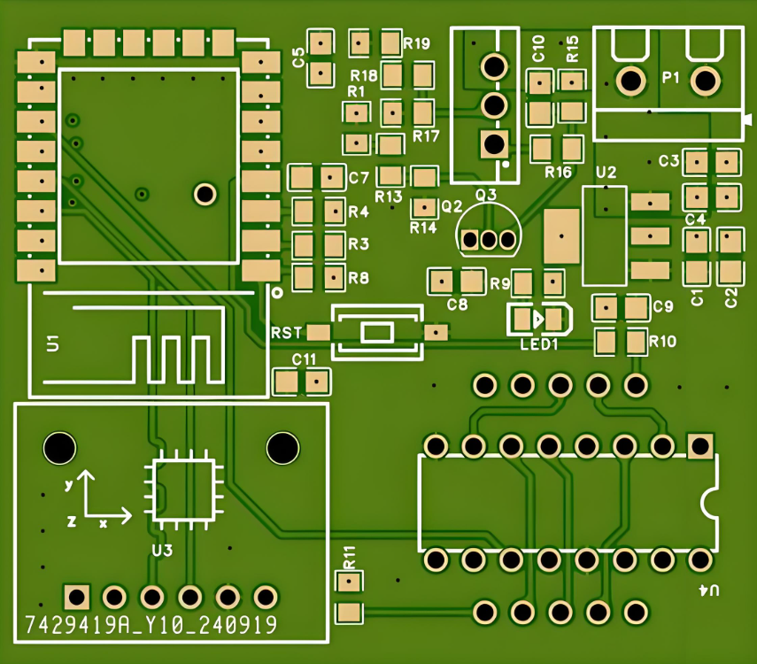
Place vias outside the pad area whenever possible. If vias-in-pad are necessary (common in high-density designs), use the smallest feasible drill size, such as 0.2 mm, and consider via filling or capping to prevent solder loss during reflow.
3. Solder Mask and Clearance
Use a solder mask defined (SMD) pad design for fine-pitch components to control solder flow. Maintain a clearance of at least 0.1 mm between the pad edge and solder mask opening to prevent bridging. For vias near pads, ensure the solder mask covers the via or use tenting to block solder paste entry.
4. Thermal Pads and Planes
For components with thermal pads (e.g., QFN packages), incorporate a grid of small vias with drill sizes of 0.3 mm or less within the pad area to dissipate heat. Space these vias evenly (e.g., 1.2 mm pitch) and fill them to avoid solder wicking.

Common Challenges and Solutions with Drill Size and SMT Pads
Even with careful planning, issues can arise when balancing drill size with SMT pad design. Here are some common problems and how to address them:
- Problem: Solder Wicking into Vias
Solution: Use smaller drill sizes (0.2-0.25 mm) and plug or tent vias to keep solder on the pad surface. - Problem: Pad Cratering During Assembly
Solution: Avoid oversized drill holes near pads and reinforce the pad with additional copper or thicker laminate materials. - Problem: Uneven Solder Paste Application
Solution: Adjust stencil apertures to reduce paste volume near vias and ensure uniform stencil thickness (e.g., 0.12 mm).
Addressing these challenges upfront during the design phase can save time and reduce rework costs during manufacturing.
How to Choose the Right Minimum Drill Size for Your Design
Selecting the optimal minimum drill size for SMT pads involves a step-by-step approach:
- Determine Component Requirements: Review the footprint and spacing needs of your SMT components to identify constraints on via placement and size.
- Assess Board Thickness: Calculate the aspect ratio for vias based on board thickness (e.g., a 1.6 mm thick board with a 0.2 mm drill size has an 8:1 ratio, which is acceptable).
- Consult Fabrication Capabilities: Confirm the smallest drill size your manufacturer can reliably produce, typically 0.2 mm for standard processes.
- Simulate Thermal and Mechanical Stress: Use design software to model heat distribution and mechanical stability around vias near SMT pads.
- Test and Iterate: Prototype your design with different drill sizes if possible, inspecting solder joints for reliability after reflow soldering.
By following these steps, you can confidently select a drill size that balances design needs with manufacturing feasibility.
Conclusion: Building Reliability into Every Solder Joint
Choosing the right minimum drill size for SMT pads is a foundational step in optimizing solder joint reliability. From influencing solder paste application to ensuring even heat distribution during reflow soldering, the drill size plays a subtle but critical role in the success of your PCB design. By adhering to PCB pad design guidelines and carefully considering factors like via placement, stencil design, and thermal management, you can create robust and reliable electronic assemblies.
Start with small drill sizes (0.2-0.3 mm) for vias near SMT pads, adjust your stencil apertures for precise solder paste deposition, and always verify your design against manufacturing constraints. With these practices, you’ll minimize defects and build PCBs that perform consistently over time.
 ALLPCB


