 ALLPCB


In the fast-paced world of defense technology, high-speed PCB (Printed Circuit Board) design plays a critical role in ensuring reliable performance of mission-critical systems. One of the biggest hurdles in this field is maintaining signal integrity, especially as data rates climb higher and devices become more compact. Signal integrity challenges in high-speed defense PCB design can lead to data errors, system failures, or compromised security if not addressed properly. This blog dives deep into these challenges, focusing on key areas like impedance control, crosstalk reduction, and EMI shielding, to help engineers design robust defense PCBs that meet stringent requirements.
Whether you’re working on radar systems, communication devices, or missile guidance technology, understanding and overcoming signal integrity issues is essential. In the sections below, we’ll explore the core challenges, practical solutions, and best practices to ensure your high-speed defense PCB design performs flawlessly under the toughest conditions.
What Is Signal Integrity and Why Does It Matter in Defense PCB Design?
Signal integrity refers to the ability of an electrical signal to travel through a PCB without distortion, interference, or loss. In high-speed defense PCB design, where signals often operate at frequencies above 1 GHz and data rates exceed 10 Gbps, maintaining signal integrity becomes a complex task. Even minor distortions can result in critical errors, potentially jeopardizing national security or mission success.
Defense applications demand exceptional reliability. A single signal glitch in a radar system could misinterpret incoming data, while interference in a communication device might disrupt secure transmissions. As a result, engineers must prioritize signal integrity to meet the strict standards of defense projects, such as MIL-STD-810 for environmental testing or MIL-PRF-31032 for PCB performance.
Key Signal Integrity Challenges in High-Speed Defense PCB Design
Designing PCBs for defense applications at high speeds introduces several unique challenges. Below, we break down the most critical issues engineers face and why they are particularly significant in defense contexts.
1. Impedance Mismatch and Control
Impedance control is a cornerstone of signal integrity in high-speed PCB design. Impedance mismatch occurs when the characteristic impedance of a transmission line doesn’t match the source or load, causing signal reflections. These reflections can distort waveforms, leading to data errors. In defense systems, where signals often travel at multi-Gbps speeds, even a small mismatch (e.g., a deviation of 5 ohms from a target 50-ohm impedance) can cause significant issues.
In defense PCB design, impedance control is complicated by the need for rugged materials and multilayer boards. For instance, high-frequency signals require consistent dielectric properties in materials like FR-4 or advanced laminates, and any variation can disrupt impedance. Additionally, tight tolerances in manufacturing are critical to maintain uniformity across traces and vias.
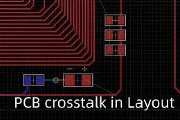
2. Crosstalk Between Traces
Crosstalk happens when a signal from one trace interferes with a neighboring trace, creating unwanted noise. In high-speed defense PCB design, where boards are densely packed with traces to save space, crosstalk is a major concern. At frequencies above 1 GHz, the electromagnetic fields around traces can couple easily, especially if traces are placed too closely together (e.g., less than 3 times the trace width apart).
In defense applications, crosstalk can corrupt sensitive data, such as encrypted communications or sensor readings. This interference not only affects performance but can also pose security risks if critical signals are misinterpreted or intercepted due to noise.
3. Electromagnetic Interference (EMI) and Shielding Issues
Electromagnetic interference (EMI) is another significant challenge in high-speed defense PCB design. EMI can originate from external sources, like nearby electronic equipment, or internally from switching power supplies and high-speed signals. Defense systems often operate in harsh environments with high levels of electromagnetic noise, making EMI shielding a top priority.
Without proper shielding, EMI can degrade signal quality, disrupt operations, or even reveal system signatures to adversaries through unintended emissions. Defense standards, such as MIL-STD-461 for electromagnetic compatibility, set strict limits on EMI, pushing engineers to design boards with robust shielding and grounding strategies.
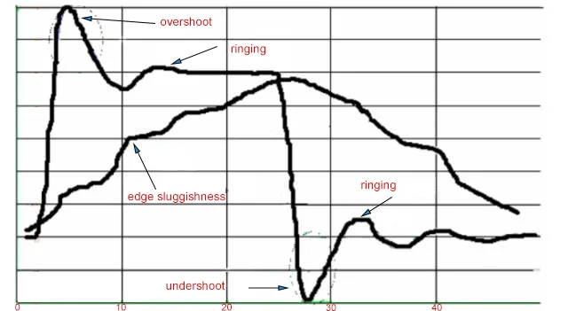
4. Signal Loss at High Frequencies
At high frequencies, signals experience greater loss due to the skin effect and dielectric losses in the PCB material. The skin effect causes current to flow only on the surface of conductors, increasing resistance, while dielectric losses occur as the PCB substrate absorbs signal energy. For defense PCBs operating at frequencies above 5 GHz, signal loss can reduce amplitude by 3 dB or more over just a few inches of trace length, leading to unreliable data transmission.
In defense systems, where long trace lengths are sometimes unavoidable due to complex layouts, minimizing signal loss is critical. Engineers must select low-loss materials and optimize trace geometries to combat this issue.
5. Power Integrity and Noise
Power integrity is closely tied to signal integrity. In high-speed defense PCB design, fluctuations in the power supply can introduce noise into signal lines, causing jitter or timing errors. Defense systems often use multiple power domains (e.g., 3.3V for digital circuits and 5V for analog components), and maintaining clean power across these domains is a challenge.
Poor power integrity can lead to system instability, especially in high-speed applications where timing precision is paramount. For example, a jitter of just 10 picoseconds in a 10 Gbps signal can result in bit errors, potentially disrupting critical operations.
Practical Solutions for Signal Integrity in Defense PCB Design
Addressing signal integrity challenges requires a combination of careful design practices, advanced materials, and simulation tools. Below are actionable strategies tailored to high-speed defense PCB design.
1. Mastering Impedance Control
To achieve precise impedance control, start by calculating the target impedance for your traces using tools like a field solver or impedance calculators. For a standard 50-ohm impedance, ensure trace width, spacing, and dielectric thickness are consistent. Use controlled impedance manufacturing processes to maintain tolerances within ±10%.
In multilayer defense PCBs, incorporate reference planes (ground or power) beneath signal layers to stabilize impedance. Also, avoid abrupt changes in trace geometry, such as sharp corners, which can cause reflections. Instead, use smooth 45-degree bends or arcs for high-speed traces.
2. Effective Crosstalk Reduction Techniques
Reduce crosstalk by increasing the spacing between high-speed traces. A general rule is to maintain a separation of at least 3 times the trace width. Additionally, route sensitive traces on different layers with a ground plane in between to act as a shield.
For differential pairs commonly used in high-speed designs, ensure equal trace lengths and consistent spacing to minimize skew and crosstalk. Use guard traces—grounded traces placed between signal lines—to further isolate critical signals in dense layouts.
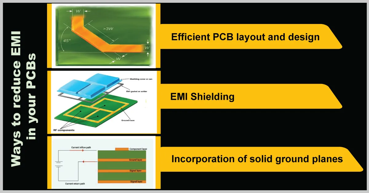
3. Implementing EMI Shielding
To combat EMI, design PCBs with solid ground planes that cover as much area as possible. Connect all ground points to a single, low-impedance ground to prevent ground loops. Use shielding cans or conductive enclosures around sensitive components to block external EMI.
Incorporate decoupling capacitors near power pins of ICs to filter out high-frequency noise. For defense applications, consider using EMI-resistant materials or coatings on the PCB to further reduce interference. Finally, follow MIL-STD-461 guidelines during testing to ensure compliance with defense standards.
4. Minimizing Signal Loss
Choose low-loss dielectric materials, such as Rogers or Isola laminates, which have a lower dielectric constant (Dk) and dissipation factor (Df) compared to standard FR-4. For example, a material with a Df of 0.002 can reduce signal loss by up to 20% at 10 GHz compared to FR-4 with a Df of 0.02.
Shorten trace lengths wherever possible and avoid unnecessary vias, as each via introduces additional loss and reflection points. When vias are needed, use back-drilling to remove unused via stubs, which can act as antennas for high-frequency signals.
5. Ensuring Power Integrity
Design a robust power distribution network (PDN) by placing decoupling capacitors close to power pins, with values ranging from 0.1 μF to 10 μF to cover a wide frequency range. Use multiple vias to connect power and ground planes, reducing impedance in the PDN.
Simulate the PDN using tools to identify resonance frequencies and adjust capacitor placement or values accordingly. A well-designed PDN can reduce voltage ripple to below 50 mV, ensuring clean power delivery to high-speed components.
Advanced Tools and Simulations for Signal Integrity
In high-speed defense PCB design, relying solely on manual calculations or rules of thumb isn’t enough. Advanced simulation tools are essential for predicting and resolving signal integrity issues before manufacturing. These tools can model impedance, crosstalk, EMI, and power integrity with high accuracy.
For instance, pre-layout simulations can help optimize trace routing and stack-up design, while post-layout analysis verifies signal performance. Tools that support 3D electromagnetic field solving are particularly useful for analyzing high-frequency effects like skin effect and dielectric loss. By integrating simulation into the design process, engineers can reduce costly redesigns and ensure compliance with defense standards.
Conclusion: Building Reliable Defense PCBs with Strong Signal Integrity
Signal integrity challenges in high-speed defense PCB design are complex but manageable with the right strategies. By focusing on impedance control, crosstalk reduction, EMI shielding, signal loss mitigation, and power integrity, engineers can create PCBs that meet the rigorous demands of defense applications. Leveraging advanced materials, precise manufacturing, and simulation tools further ensures success in this critical field.
At every stage of the design process, prioritizing signal integrity isn’t just about performance—it’s about ensuring the safety, security, and reliability of systems that protect lives and nations. With careful planning and attention to detail, your high-speed defense PCB designs can achieve the robustness needed to excel in the most challenging environments.


