 ALLPCB


If you're looking to improve your Printed Circuit Board (PCB) design, understanding PCB ground planes is essential. A ground plane is a large area of copper on a PCB that serves as a common reference point for electrical signals, helping to reduce electromagnetic interference (EMI) and enhance signal integrity. In this comprehensive guide, we'll dive deep into the benefits of ground planes, how they help with EMI reduction, and provide a detailed design guide to ensure your circuits perform at their best.
What Is a PCB Ground Plane and Why Does It Matter?
A PCB ground plane is a layer of copper within or on the surface of a circuit board that acts as a common ground reference for all components. It provides a low-impedance path for return currents, stabilizes voltage levels, and minimizes noise in the circuit. Without a proper ground plane, your PCB could suffer from issues like signal distortion, crosstalk, and excessive EMI, which can disrupt the performance of sensitive electronics.
Ground planes are especially critical in high-speed digital and analog designs where signal integrity and noise reduction are top priorities. By incorporating a well-designed ground plane, you can significantly improve the reliability and efficiency of your board. Let’s explore the key benefits and design principles to help you master this essential aspect of PCB layout.

Key Benefits of PCB Ground Planes
Understanding the advantages of ground planes is the first step in leveraging their potential. Below, we break down the primary benefits that make ground planes a must-have in modern PCB designs.
1. EMI Reduction with Ground Plane
Electromagnetic interference (EMI) occurs when unwanted electrical noise disrupts the operation of electronic devices. A ground plane acts as a shield, reducing EMI by providing a low-impedance path for return currents. This prevents the currents from forming large loops that radiate electromagnetic fields. Studies have shown that a solid ground plane can reduce radiated EMI by up to 20 dB in high-frequency circuits, ensuring compliance with strict regulatory standards.
For example, in a 4-layer PCB design, placing a continuous ground plane beneath signal traces can effectively suppress noise from high-speed signals, such as those running at 100 MHz or higher. This makes ground planes indispensable for applications like wireless communication and automotive electronics, where EMI can cause critical failures.
2. Signal Integrity with Ground Plane
Signal integrity refers to the quality and reliability of electrical signals as they travel through a circuit. A ground plane helps maintain signal integrity by providing a consistent reference voltage and minimizing impedance mismatches. For high-speed signals, such as those in DDR memory interfaces operating at 1 GHz, a ground plane can reduce signal reflections and crosstalk by ensuring return currents follow the shortest path beneath the signal trace.
Without a ground plane, signal traces may experience voltage drops or noise pickup, leading to data errors. A well-implemented ground plane ensures cleaner, more stable signals, which is vital for high-performance designs.
3. Improved Power Distribution
Ground planes work hand-in-hand with power planes to create a low-impedance power distribution network. This reduces voltage fluctuations and ensures that components receive stable power. For instance, in a design with multiple ICs drawing transient currents, a ground plane can prevent voltage sags by evenly distributing return currents across the board.
4. Thermal Management
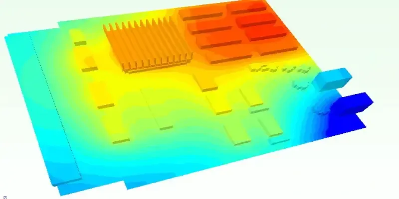
A ground plane also aids in heat dissipation by spreading thermal energy across a large copper area. This is especially useful in power electronics where components like MOSFETs generate significant heat. A ground plane can lower the thermal resistance of the board, helping to maintain safe operating temperatures.
Related Reading: The Ultimate Guide to PCB Ground Planes: Boost Signal Integrity and Reduce EMI
Ground Plane Design Guide: Best Practices for Optimal Performance
Now that we’ve covered the benefits, let’s dive into a practical PCB ground plane tutorial. These design tips will help you create boards that maximize signal integrity and minimize EMI.
1. Use a Continuous Ground Plane
Whenever possible, dedicate an entire layer of your PCB to a solid, unbroken ground plane. Breaks or splits in the ground plane can create high-impedance paths for return currents, leading to increased noise and EMI. In a 4-layer board, for example, reserve the second layer as a continuous ground plane to provide a reference for signal layers above and below.
If splits are unavoidable due to mixed-signal designs (e.g., analog and digital sections), ensure they are strategically placed and bridged with capacitors to maintain a low-impedance connection at high frequencies.
2. Minimize Return Path Interruptions
Return currents should follow the path of least resistance, ideally directly beneath the signal trace. Avoid routing signal traces over splits or gaps in the ground plane, as this forces return currents to take longer, noisier paths. For high-speed signals like USB 3.0 operating at 5 Gbps, even a small interruption in the return path can degrade signal quality.
Use vias sparingly and place them close to signal transitions between layers to keep return paths short. Tools like simulation software can help visualize return current paths during the design phase.
3. Separate Analog and Digital Grounds (When Necessary)
In mixed-signal designs, separating analog and digital grounds can prevent noise from digital circuits from interfering with sensitive analog components. However, these grounds should be connected at a single point near the power supply to avoid creating ground loops. This technique is common in audio amplifier designs where analog signals need protection from digital switching noise.
4. Place Decoupling Capacitors Close to ICs
Decoupling capacitors stabilize the power supply by filtering out noise, but their effectiveness depends on placement. Position them as close as possible to the power pins of ICs, with short traces to the ground plane. For a microcontroller operating at 50 MHz, a 0.1 μF capacitor placed within 0.1 inches of the power pin can significantly reduce noise spikes.
5. Avoid Overlapping High-Speed Signals Without a Ground Reference
In multilayer boards, ensure high-speed signal traces are routed adjacent to a ground plane. If a signal layer is sandwiched between two power planes without a ground reference, it can lead to crosstalk and EMI. Always maintain a ground plane as the reference layer for critical signals to keep impedance controlled—typically around 50 ohms for most high-speed designs.
Related Reading: Mastering PCB Inner Layer Stackup: Optimizing Power and Ground Planes
Common Ground Plane Mistakes to Avoid
Even with the best intentions, certain design errors can undermine the effectiveness of a ground plane. Here are some pitfalls to watch out for during your PCB layout process.
1. Using Copper Pours Instead of a Solid Plane
While copper pours (small patches of copper) can help with grounding in simple designs, they are no substitute for a solid ground plane. Pours often have gaps or irregular shapes, leading to inconsistent return paths and increased EMI. Always opt for a dedicated, continuous ground layer in complex or high-speed designs.
2. Ignoring Ground Plane Stitching
In multilayer boards, ground planes on different layers should be connected using stitching vias. Without proper stitching, isolated ground areas can act as antennas, radiating noise. Place vias at regular intervals (e.g., every 0.5 inches) around the board’s perimeter to ensure a uniform ground potential.
3. Overloading the Ground Plane with Signals
Never route signal traces or power lines through a ground plane layer. This disrupts the continuity of the plane and creates noise. Reserve the ground layer exclusively for grounding to maintain its effectiveness.
Advanced Tips for EMI Reduction with Ground Planes
For designs that demand the highest levels of EMI suppression, consider these advanced strategies to take your ground plane implementation to the next level.
1. Implement a Ground Grid for Large Boards
In very large PCBs, a single ground plane may not be feasible due to cost or layer constraints. In such cases, a ground grid—a network of interconnected ground traces—can approximate the benefits of a solid plane. Ensure the grid spacing is small enough (e.g., less than 1/20th of the wavelength of the highest frequency signal) to prevent EMI radiation.
2. Use Multiple Ground Planes in High-Frequency Designs
For RF applications operating at frequencies above 1 GHz, multiple ground planes can provide additional shielding. Stack ground planes between signal layers to isolate high-frequency signals and reduce crosstalk. This approach is common in microwave circuit designs where signal isolation is critical.
3. Shield Sensitive Areas with Ground Vias
Surround sensitive components or traces with a ring of ground vias connected to the ground plane. This creates a Faraday cage effect, blocking external EMI from interfering with critical signals. This technique is often used in wireless modules to protect RF signals from external noise sources.
How to Test and Validate Your Ground Plane Design
After designing your ground plane, validation is key to ensuring it performs as expected. Use the following methods to test your PCB for signal integrity and EMI issues.
1. Simulate Return Paths
Use PCB design software with simulation capabilities to model return current paths. This helps identify potential bottlenecks or interruptions in the ground plane that could affect performance.
2. Measure EMI Emissions
Conduct EMI testing using a spectrum analyzer to measure radiated emissions from your board. Compare the results against regulatory standards (e.g., FCC or CISPR) to ensure compliance. If emissions are high, revisit your ground plane design for gaps or splits.
3. Check Signal Integrity with an Oscilloscope
Use an oscilloscope to analyze signal waveforms for noise, overshoot, or ringing. For a high-speed signal like PCIe at 2.5 Gbps, clean waveforms indicate a well-designed ground plane with minimal impedance mismatches.
Conclusion: Mastering PCB Ground Planes for Superior Designs
PCB ground planes are a cornerstone of effective circuit design, offering unmatched benefits for signal integrity and EMI reduction. By following the best practices outlined in this ground plane design guide, you can create boards that perform reliably even in demanding applications. From using continuous ground layers to avoiding common mistakes like improper via placement, every detail matters in achieving optimal results.
Whether you're a beginner seeking a PCB ground plane tutorial or an experienced engineer looking to refine your skills, these strategies will help you build better circuits. Implement these tips in your next project to boost performance, reduce noise, and ensure your designs stand out for their quality and reliability.
With the right approach to ground plane design, you’re well on your way to mastering the art of PCB layout. Keep experimenting, testing, and refining your techniques to stay ahead in the ever-evolving world of electronics design.


