ALLPCB


FR 4 PCB Layer Stackup Design: Best Practices and Optimization
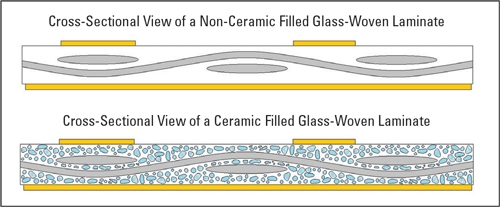
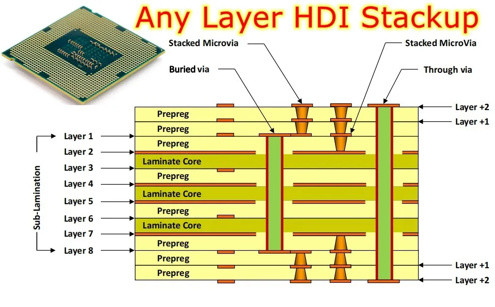
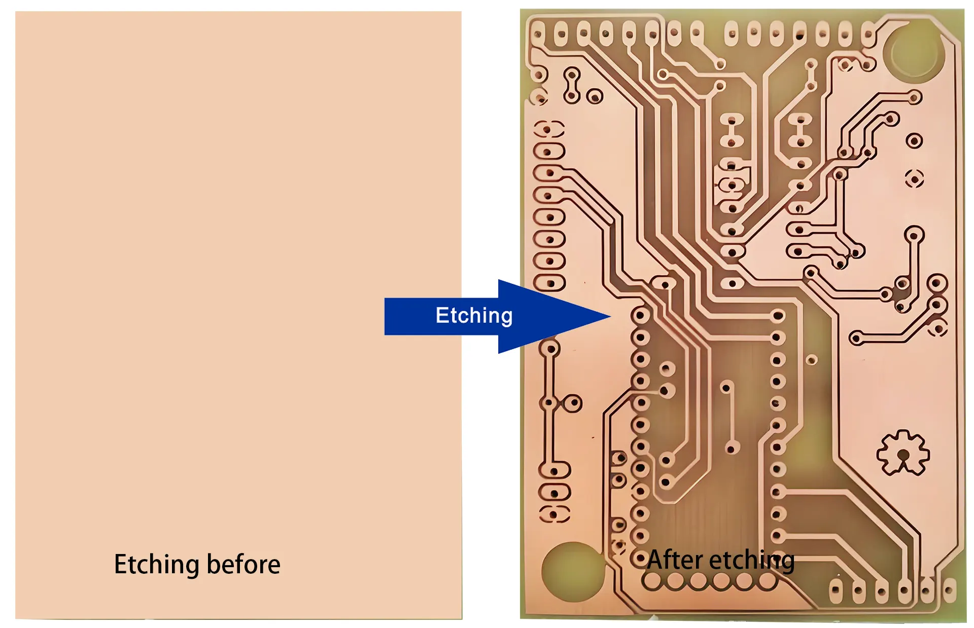
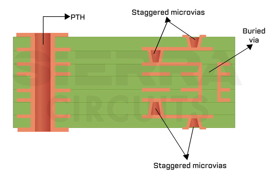
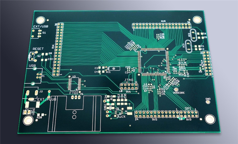
FR-4 PCB layer stackup best practices cover impedance control stackups, power and ground plane design, and signal layer routing rules for multilayer FR-4 PCB design. Electric engineers apply these guidelines to prevent warpage, reduce crosstalk, and achieve reliable high-speed performance in complex boards.