 ALLPCB


Introduction
Reflow soldering stands as a cornerstone process in surface mount technology assembly, particularly for high-volume production where consistency and reliability are paramount. This method involves controlled heating to melt solder paste, forming robust electrical and mechanical connections between components and the printed circuit board. In high-volume PCB assembly, mastering reflow soldering balances the art of precise process control with the science of thermal dynamics and material behavior. Engineers must navigate variables like oven configuration and material interactions to achieve defect-free results. The process demands attention to detail, as even minor deviations can lead to failures in the field. Understanding reflow soldering empowers electric engineers to optimize production lines for efficiency and quality.
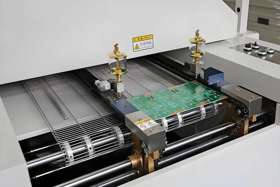
What Is Reflow Soldering and Why It Matters in High-Volume PCB Assembly
Reflow soldering refers to the thermal process where solder paste, applied to PCB pads, transitions through phases of heating to form reliable joints without manual intervention. The sequence includes preheating to activate flux, soaking to stabilize temperatures, reflowing to liquefy the solder alloy, and controlled cooling to solidify connections. In high-volume environments, this automated process enables rapid throughput while maintaining uniformity across thousands of boards. Poor reflow execution risks defects like voids or bridges, compromising signal integrity and mechanical strength. For electric engineers, it matters because reflow directly impacts yield rates, rework costs, and long-term product reliability in demanding applications. Adhering to standards like IPC J-STD-001J ensures processes meet industry benchmarks for soldered assemblies.
The relevance amplifies in surface mount technology, where component density challenges traditional soldering methods. High-volume lines rely on conveyorized ovens to handle diverse board sizes and complexities consistently. Engineers prioritize reflow to minimize variability from board-to-board, especially with mixed component types. This process also accommodates lead-free alloys, aligning with environmental regulations without sacrificing performance. Ultimately, effective reflow soldering scales production while upholding quality control.
The Technical Principles of Reflow Soldering
At its core, reflow soldering hinges on the phase changes of solder paste, a mixture of flux, alloy particles, and activators. During heating, flux removes oxides, allowing the alloy to melt and wet the pads and terminations uniformly. Solder paste melting PCB occurs precisely in the reflow zone, where surface tension pulls the liquid solder into a concave fillet for optimal joint formation. Thermal gradients across the board influence this wetting, demanding controlled heat transfer to prevent distortions. Electric engineers analyze these principles to predict joint microstructure and intermetallic growth.
Heat transfer in reflow ovens primarily uses forced convection, ensuring even distribution in multi-zone setups. Radiation and conduction play secondary roles, but convection dominates for high-volume consistency. The process follows a defined thermal profile to match alloy melting characteristics and component tolerances. Deviations can alter flux activity or cause incomplete melting, leading to weak joints. Profiling tools verify that the board experiences the intended ramp rates and peak exposures.
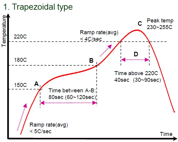
IPC-7530A provides guidelines for developing these profiles, emphasizing test vehicle construction and data analysis techniques.
Reflow Oven Set Up for PCB Assembly
Proper reflow oven set up PCB begins with zone configuration tailored to the thermal mass of the assembly. Multiple heating and cooling zones allow independent control of ramp rates and dwell times, critical for high-volume runs. Conveyor speed calibration ensures residence time matches the profile, preventing under or overexposure. Nitrogen atmosphere options reduce oxidation in sensitive alloys, enhancing joint cosmetics and reliability. Engineers verify setup using loaded board simulations to account for real-world heat sinks like large components.
SMT reflow soldering machine maintenance involves regular calibration of fans, heaters, and exhaust systems for uniform airflow. Belt tension and height adjustments accommodate various PCB thicknesses without sagging. Software interfaces enable recipe storage for quick changeovers between products. Initial runs include empty oven profiling to baseline performance before production. Troubleshooting airflow imbalances early avoids hot spots that plague high-volume output.
Zone sequencing starts with preheat for flux activation, followed by soak for solvent evaporation and temperature uniformity. Reflow zone peaks align with alloy liquidus, while cooling prevents thermal shock. Documenting setup parameters facilitates repeatability across shifts.
Temperature Profiling in PCB Manufacturing
Temperature profiling PCB validates that every board follows the optimal thermal trajectory during reflow. Engineers attach thermocouples to critical locations, such as thick copper areas, component bodies, and board edges, then run a test assembly through the oven. Data loggers capture real-time curves, overlaid against target profiles for delta analysis. This practice identifies issues like insufficient soak or excessive peaks before full production. Regular profiling, at least weekly or per product change, maintains process stability in high-volume lines.
Profiling reveals board-level variations due to thickness, copper density, or component shadowing. Adjustments to oven setpoints compensate for these, ensuring solder paste melting PCB occurs simultaneously across joints. J-STD-020F outlines reflow conditions for moisture-sensitive devices, guiding profile limits to avoid package damage. Visualizing data trends helps predict defect correlations, streamlining troubleshooting.
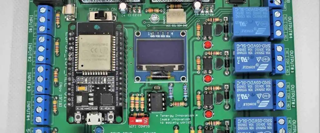
Advanced profilers offer wireless options for multi-channel monitoring, reducing setup time.
Best Practices for High-Volume SMT Reflow Soldering
Implement standardized recipes per alloy type and board family to streamline reflow oven set up PCB. Preheat ramps should be gradual to minimize thermal stress, while soak durations allow flux to fully activate without drying out. Reflow peaks must exceed liquidus sufficiently for complete melting, followed by rapid yet controlled cooling to form fine grain structures. Monitor conveyor loading to avoid heat overload, spacing boards adequately for airflow.
Stencil printing precision ensures uniform solder paste volume, critical for consistent melting. Component placement accuracy, within tolerances, prevents offsets that exacerbate defects. Oven cleanliness prevents flux residue buildup, which alters heat transfer. Data-driven adjustments from profiling refine practices iteratively.
Integrate inline monitoring for real-time feedback, halting lines on profile excursions.
Troubleshooting Common Issues: Minimizing Tombstoning in PCB Assembly
Tombstoning manifests as components standing upright on one end, often disrupting electrical continuity in fine-pitch parts. Primary causes include uneven solder paste melting PCB, where one pad wets before the other due to thermal gradients or volume imbalances. Pad design asymmetry or poor solderability amplifies torque forces during reflow. Placement inaccuracies shift mass centers, promoting lift-off.
Minimizing tombstoning PCB assembly starts with balanced paste deposition via optimized stencils and printing parameters. Slower preheat ramps equalize temperatures across terminations, delaying differential melting. Profile verification confirms uniform heating, adjusting zones as needed. Pad sizing per IPC J-STD-001J promotes even wetting without excess solder on one side.
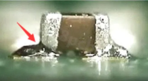
Secondary checks include flux compatibility and board warpage, which distort joints. Post-reflow inspection quantifies incidence, correlating to process tweaks. Consistent practices yield rates above industry norms.
Other defects like head-in-pillow trace to insufficient reflow peaks or oxide entrapment, resolved via extended dwells.
Conclusion
Reflow soldering masterfully combines thermal science with practical execution to drive high-volume PCB assembly success. Key to excellence lies in meticulous reflow oven set up PCB, rigorous temperature profiling PCB, and proactive defect mitigation like minimizing tombstoning PCB assembly. Electric engineers leveraging these insights achieve superior yields and reliability. Standards guide but hands-on profiling and troubleshooting refine the process uniquely per line. Embracing this art and science elevates production from good to exceptional.
FAQs
Q1: How do you set up a reflow oven for PCB assembly in high-volume production?
A1: Reflow oven set up PCB involves configuring zones for preheat, soak, reflow, and cooling based on alloy and board specs. Calibrate conveyor speed and airflow for uniform heat, then profile with thermocouples on a test board. Verify against target curves, adjusting setpoints for consistency. Maintenance like cleaning heaters prevents drift. This ensures reliable SMT reflow soldering machine performance across runs.
Q2: What is temperature profiling in PCB reflow soldering?
A2: Temperature profiling PCB captures actual thermal exposure during reflow using sensors on assemblies. It validates preheat ramps, soak stability, reflow peaks, and cooling rates match requirements. Engineers analyze deltas to tweak oven settings, preventing defects from underheating or overheating. Regular profiling maintains process windows for varying board types. Essential for high-volume quality control.
Q3: How does solder paste melting occur in the reflow process?
A3: Solder paste melting PCB happens in the reflow zone after flux activation and soak. Gradual heating liquefies the alloy, enabling wetting via surface tension. Uniform volume and profiles ensure simultaneous melting on both terminations. Imbalances lead to defects like incomplete joints. Profiling confirms optimal conditions per IPC-7530A guidelines.
Q4: What are effective ways to minimize tombstoning in PCB assembly?
A4: Minimizing tombstoning PCB assembly requires balanced solder paste volumes and precise placement. Optimize reflow profiles with slow ramps for even heating across pads. Verify pad designs promote symmetric wetting. Profile regularly to eliminate thermal gradients. These steps reduce lift-off risks in fine-pitch components effectively.
References
IPC J-STD-001J — Requirements for Soldered Electrical and Electronic Assemblies. IPC, 2024
IPC-7530A — Guidelines for Temperature Profiling for Mass Soldering Processes (Reflow and Wave). IPC, 2017
IPC/JEDEC J-STD-020F — Moisture/Reflow Sensitivity Classification for Non-Hermetic Surface Mount Devices. IPC/JEDEC, 2022





