 ALLPCB


Introduction
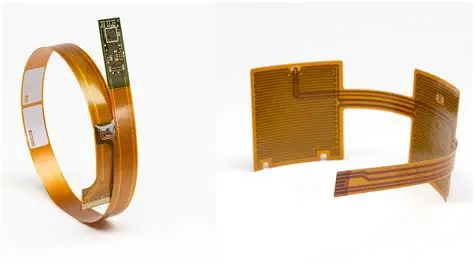
Flex and rigid-flex printed circuit boards represent advanced solutions for modern electronics where space constraints and mechanical flexibility are critical. These designs allow devices to fit into tight enclosures, withstand vibrations, and enable innovative form factors in applications like wearables, medical implants, and aerospace systems. However, achieving efficient batch manufacturing requires careful attention to flex PCB design principles that minimize defects and maximize yield. Poor design choices can lead to issues such as cracking during bending or delamination in production, inflating costs and delaying timelines. By prioritizing design for manufacturability (DFM) from the outset, engineers can streamline rigid-flex PCB manufacturing processes, ensuring high-volume production runs with consistent quality. This article explores the technical foundations, best practices, and assembly considerations tailored for electrical engineers seeking reliable batch outcomes.
Understanding Flex and Rigid-Flex PCBs: Definitions and Industry Relevance
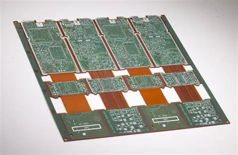
Flex PCBs consist entirely of flexible substrates, conductors, and coverlayers, allowing repeated bending without structural failure. In contrast, rigid-flex PCBs combine rigid sections made from standard epoxy-based laminates with flexible interconnects, providing mechanical support for components while maintaining interconnect flexibility. These hybrid boards are essential in industries demanding compact, lightweight assemblies, such as consumer electronics and automotive sensors, where traditional rigid boards fall short. For batch manufacturing, their relevance lies in enabling economies of scale through panelized production, where multiple units are fabricated simultaneously to reduce per-unit costs. Designing for these formats ensures compatibility with standard high-volume processes like lamination, etching, and plating. Ultimately, proper implementation supports faster time-to-market and higher reliability in demanding environments.
Core Technical Principles in Flex PCB Design
The foundation of effective flex PCB design begins with understanding layer stackups and material interactions under mechanical stress. Flexible substrates typically use polyimide films for their high thermal stability and ductility, paired with rolled annealed copper foil to prevent cracking during flexure. Coverlays protect traces and provide insulation, while adhesives bond layers without compromising bend performance. In rigid-flex designs, transitions between rigid and flex zones demand precise control of material thicknesses to avoid stress concentrations. Trace routing in flex areas must follow curved paths aligned with the bend axis, minimizing grain direction effects on copper ductility. Adherence to IPC-2223 guidelines ensures these principles translate to robust designs suitable for production scaling.
Bend radius represents a critical parameter in flex PCB design, dictating the minimum curvature without inducing fatigue or fractures. For static applications, where bending occurs once during installation, the radius is generally set at least six to ten times the total stackup thickness for single- or double-sided boards. Dynamic applications, involving repeated flexing, require significantly larger radii, often 30 times or more, to achieve cycle life in the millions. Factors like copper weight and layer count influence these values, with heavier foils demanding gentler curves. Engineers must simulate these in design software to predict stress distribution. Consistent application prevents common failures like trace micro-cracks observed in accelerated life testing.
Material Selection Strategies for Flex and Rigid-Flex PCBs
Material selection profoundly impacts both performance and manufacturability in rigid-flex PCB manufacturing. Polyimide remains the preferred dielectric for flex sections due to its low moisture absorption, wide operating temperature range, and excellent chemical resistance. For rigid portions, glass-reinforced epoxy laminates provide the necessary rigidity and hole wall integrity for through-hole components. Adhesive systems, such as acrylic or modified epoxy, must balance bond strength with peel flexibility to prevent delamination during thermal cycling. Coverlay materials mirror substrate choices, often polyimide-based, to ensure uniform thickness and adhesion. Engineers should evaluate CTE mismatch between materials to minimize warpage in multi-layer builds.
Stiffeners, typically FR4 or polyimide sheets, add local rigidity for connectors or heavy components without altering flex zones. Copper foil type—electrodeposited for rigid areas, rolled for flex—optimizes etch uniformity and bend endurance. Surface finishes like ENIG or OSP influence solderability during PCB assembly, with flex areas favoring immersion tin for its ductility. Selecting materials compliant with IPC-6013 qualification requirements guarantees performance under environmental stresses. Batch efficiency improves with standardized material sets available in large volumes, reducing lead times and variability.
Best Practices for Design for Manufacturability in Batch Production
Efficient batch manufacturing hinges on panelization strategies that maximize material utilization and automate handling. Designers should array multiple flex or rigid-flex units on carrier panels with breakaway tabs, incorporating tooling holes and fiducials for precise registration during etching and assembly. Standard panel dimensions facilitate high-throughput lamination presses and exposure equipment. Avoiding non-standard features like odd-shaped outlines or excessive copper imbalances prevents yield losses from warpage or plating voids. Flex tails should terminate with straight edges for easy singulation post-fabrication.
In flex PCB design, routing traces parallel to the bend axis and using teardrops at pads reduces stress risers. Vias in flex zones should be minimized or replaced with flying leads to avoid barrel cracking. For rigid-flex PCB manufacturing, bookbinding construction—laminating flex cores between rigid multilayers—enhances yield by sequential processing. Component placement must keep high-density areas on rigid sections, with clearances of at least 0.5 mm from flex boundaries. These practices align with factory workflows, enabling parallel processing of hundreds of panels.
Layer count optimization streamlines pressing cycles; combining signals where possible cuts costs without sacrificing integrity. Ground planes in flex areas should use hatched patterns to relieve stress, while solid fills suit rigid zones. Solder mask and silkscreen registration tolerances tighten for batch laser plotting. Pre-verifying designs against DFM checklists catches issues early, boosting first-pass yields above 95% in volume runs.
PCB Assembly Considerations for Flex and Rigid-Flex Boards
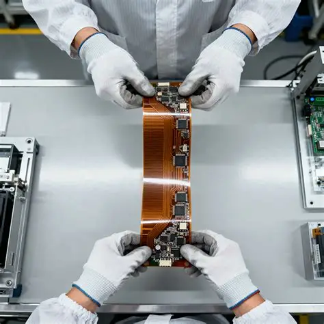
PCB assembly for flex and rigid-flex boards demands adaptations to handle variable geometries. Surface mount technology (SMT) processes treat rigid sections conventionally, using stencils optimized for planar areas. Flex tails require protective fixtures during reflow to prevent unintended bending, with peak temperatures controlled per component specifications. Through-hole components on rigid-flex benefit from wave soldering, but flux residues must be cleaned to avoid ionic contamination in flex dielectrics.
Stiffeners attach post-assembly via adhesive or mechanical fasteners, providing leverage points for connectors. Inspection follows IPC-A-610 criteria, emphasizing bend areas for microcracks via cross-sectioning or dye penetrant. Automated optical inspection (AOI) verifies fiducials and traces before folding. For batch efficiency, grouping assemblies by flex configuration minimizes changeover times on pick-and-place machines. Troubleshooting common issues like tombstoning involves adjusting stencil apertures and paste volumes tailored to uneven surfaces.
Troubleshooting Common Issues in Production
Design flaws often manifest as flex tail delamination or rigid-flex transition fractures during high-volume runs. Warpage from asymmetric stackups corrects via balanced copper distribution or carrier clamping in lamination. Excessive bend radius violations lead to field failures; iterative FEA modeling refines curves pre-production. Material inconsistencies cause plating adhesion failures, resolved by specifying foil treatments. Panel-level bow monitoring during etching prevents downstream misalignment. Proactive root cause analysis using failure modes like IPC-6013 testing protocols elevates batch reliability.
Conclusion
Designing flex and rigid-flex PCBs for efficient batch manufacturing integrates precise flex PCB design, strategic material selection, and assembly-aware layouts. Key elements like bend radius optimization, stackup balancing, and DFM panelization directly drive yield and cost savings. Electrical engineers benefit from standards-guided approaches that ensure mechanical integrity alongside electrical performance. Implementing these practices positions products for scalable production, reducing risks in dynamic applications. Future designs will leverage evolving materials while upholding proven principles for sustained success.
FAQs
Q1: What role does bend radius play in flex PCB design for reliable performance?
A1: Bend radius is crucial in flex PCB design as it determines the minimum curvature traces and substrates can endure without cracking or fatigue. Per industry guidelines, static bends require 6-10 times the stackup thickness, while dynamic needs 30 times or more. Undersizing leads to early failures in repeated flexing scenarios. Engineers calculate it factoring copper weight and layer count, simulating stress for validation. Proper sizing enhances batch yields by minimizing rejects during qualification testing.
Q2: How should material selection influence rigid-flex PCB manufacturing processes?
A2: Material selection in rigid-flex PCB manufacturing balances flexibility, rigidity, and thermal compatibility. Polyimide suits flex zones for ductility, while epoxy laminates reinforce rigid areas. Adhesives must match CTE to prevent delamination under reflow. Standardizing choices streamlines procurement for batches, cutting lead times. Evaluate per application demands like temperature and humidity for optimal stackups. This approach ensures high-volume compatibility and reliability.
Q3: What are key considerations for PCB assembly of flex and rigid-flex boards?
A3: PCB assembly for flex and rigid-flex boards requires fixtures to maintain flatness during SMT reflow and prevent flex damage. Place components on rigid sections, using tailored stencils for uneven surfaces. Post-assembly stiffeners aid handling and connectors. IPC-A-610 inspection focuses on bend zones for defects. Automating fiducial alignment boosts batch throughput. These steps minimize handling errors and support high yields.
Q4: Why prioritize DFM in flex PCB design for batch manufacturing efficiency?
A4: DFM in flex PCB design optimizes panelization, trace routing, and feature standardization for batch manufacturing. It avoids custom tooling by using standard outlines and clearances, enabling parallel processing. Bend radius and material choices reduce defects like warpage. Fiducials ensure precise registration in etching and assembly. This holistic approach lowers costs per unit and accelerates production ramps for electrical engineers.


