ALLPCB


Introduction
Polyimide PCBs represent a critical advancement in printed circuit board technology, particularly for applications demanding exceptional thermal stability and mechanical flexibility. These boards utilize polyimide substrates that withstand extreme temperatures, often exceeding 200 degrees Celsius, making them ideal for aerospace, automotive, and military electronics. Manufacturing polyimide PCBs requires precision at every stage to maintain signal integrity and reliability under harsh conditions. This guide outlines the complete fabrication process, focusing on key procedures like the polyimide PCB lamination process, polyimide PCB drilling techniques, and polyimide PCB surface finish options. Engineers benefit from understanding these steps to optimize designs for high-performance environments. Factory insights reveal that adherence to controlled parameters minimizes defects such as delamination or warpage.
What Are Polyimide PCBs and Why Do They Matter?
Polyimide PCBs employ polyimide resin as the core dielectric material, offering superior thermal resistance compared to standard FR-4 laminates. This polymer exhibits a glass transition temperature above 250 degrees Celsius, low thermal expansion, and excellent chemical stability. In multilayer configurations, polyimide enables rigid-flex or fully flexible boards that bend without compromising conductivity. Their relevance stems from demanding sectors where conventional materials fail, such as downhole oil exploration or space systems. Engineers specify polyimide for its ability to endure vibration, humidity, and repeated thermal cycling. Production challenges arise from the material's toughness, necessitating specialized processes to achieve high yields.
Key Materials in Polyimide PCB Fabrication
Core materials include polyimide films or prepregs, copper foil, and adhesives for bonding. Polyimide films provide the base substrate, available in adhesiveless configurations to enhance peel strength. Copper foil, typically electrodeposited, ranges from 1/2 oz to 2 oz per square foot for fine-line circuitry. Prepregs incorporate polyimide resin impregnated into glass fabric for multilayer builds. Surface treatments like brown oxide promote adhesion during lamination. Selection aligns with IPC-4101 specifications for base materials, ensuring consistent dielectric properties and thermal performance.
The Polyimide PCB Manufacturing Process
Step 1: Design and Material Preparation
Fabrication begins with Gerber file review and design for manufacturability analysis. Engineers verify trace widths, via sizes, and bend radii to suit polyimide's properties. Materials undergo incoming inspection for thickness uniformity and moisture content. Baking at controlled temperatures removes absorbed moisture, preventing voids during subsequent heating. Panels cut from polyimide sheets prepare for inner layer processing. This preparation sets the foundation for reliable interlayer connections.
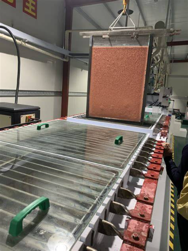
Step 2: The Polyimide PCB Lamination Process
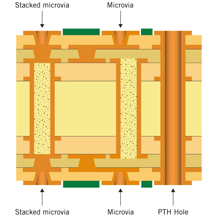
The polyimide PCB lamination process bonds copper foil to polyimide substrates under vacuum to eliminate air pockets. Inner layers receive brown oxide treatment to create a micro-rough surface for improved adhesion. Stacked layers enter a vacuum press or autoclave, where temperatures reach 350 degrees Celsius and pressures up to 500 psi cure the resin fully. Cycle times extend to several hours, allowing gradual heating to control flow and avoid resin squeeze-out. Post-lamination, boards cool slowly under pressure to minimize warpage. This step demands precise tooling holes for alignment in multilayer builds.
Sequential lamination builds complex structures by laminating rigid sections first, then flex cores. Factory protocols monitor pressure uniformity across panels. Deviations lead to inconsistent bond lines, compromising mechanical integrity.
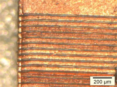
Step 3: Polyimide PCB Drilling Techniques
Polyimide PCB drilling techniques address the material's abrasiveness and heat sensitivity. Mechanical drilling uses carbide bits with high helix angles and peck cycles to clear chips and reduce heat buildup. Laser drilling, employing UV or CO2 lasers, excels for microvias under 100 microns, ablating polyimide cleanly without burrs. Plasma desmear follows to remove residue, as chemical etchants prove too aggressive for polyimide. Aspect ratios typically limit to 1:1 for mechanical holes due to drill wander risks. Optical inspection verifies hole registration post-drilling.
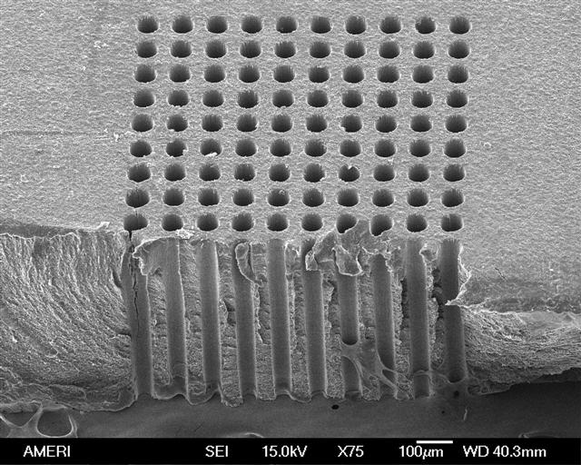
In accordance with IPC-6013 qualification standards for flexible boards, hole wall quality must exhibit smooth profiles free of cracks. Engineers select techniques based on via density and board thickness.
Step 4: Electroless Plating and Pattern Plating
Holes receive electroless copper deposition to initiate barrel plating, typically 0.5 to 1 micron thick. Pattern plating builds up copper to 25 microns on traces and vias using electrolytic baths. Current density controls uniform thickness, avoiding dog-boning in high-aspect holes. Racks ensure even electrolyte flow around flex sections. This metallization enables reliable interlayer vias. Post-plating, flash etching smooths surfaces.
Step 5: Imaging, Etching, and Stripping
Dry film photoresist applies to outer layers, exposed via artwork, and developed to define circuitry. Differential etching removes unwanted copper using alkaline or cupric chloride solutions. Tin or nickel etch resist protects traces during this step. Stripping removes resist, revealing fine-line patterns down to 50 microns. Plasma cleaning enhances solder mask adhesion afterward. Process controls prevent under-etching, critical for polyimide's thermal expansion mismatch with copper.
Step 6: Solder Mask and Coverlay Application
Coverlay films, polyimide-based with adhesive, laminate over flex areas for insulation and protection. Screen-printed solder mask covers rigid sections, cured via UV or thermal ovens. Laser trimming defines outlines precisely. This dual protection suits rigid-flex hybrids. Alignment fiducials ensure registration accuracy.
Step 7: Polyimide PCB Surface Finish Options
Polyimide PCB surface finish options prioritize solderability and environmental resistance. Electroless Nickel Immersion Gold (ENIG) deposits 3-5 microns nickel under 0.05 micron gold, ideal for fine-pitch leads due to flatness. Organic Solderability Preservative (OSP) applies a thin organic coating, cost-effective for high-volume but sensitive to handling. Immersion Tin offers 0.8-1.2 microns tin for press-fit pins, while Hard Gold suits high-wear contacts. Selection depends on assembly method and shelf life requirements. ENIG prevails in high-reliability applications for its wire bond compatibility.
Step 8: Electrical Testing and Final Inspection
Flying probe or bed-of-nails testers verify continuity and shorts per netlist. Impedance testing confirms controlled lines for high-speed signals. Visual and automated optical inspection detect defects like mouse bites. Warpage measurement ensures flatness within limits. Final routing and scoring prepare for assembly. Certification to IPC-A-600 acceptability criteria confirms quality.
Best Practices for Polyimide PCB Manufacturing
Maintain cleanroom conditions to prevent contamination during lamination. Implement bake-out protocols before each thermal step, targeting less than 0.1% moisture. Use fiducial marks for multilayer alignment, tolerating no more than 50 microns shift. Monitor drill bit wear hourly, replacing at predefined flute lengths. Validate surface finishes via wettability tests post-application. Sequential builds reduce stress concentrations in rigid-flex transitions.
Conclusion
Polyimide PCB manufacturing demands meticulous control over lamination, drilling, and finishing to deliver boards for extreme environments. The polyimide PCB lamination process ensures robust interlayer bonds, while specialized polyimide PCB drilling techniques enable dense interconnects. Diverse polyimide PCB surface finish options tailor protection to assembly needs. Engineers gain reliability by integrating these steps with standard-aligned practices. Future designs will leverage polyimide's versatility for ever-harsher applications.
FAQs
Q1: What is the polyimide PCB lamination process?
A1: The polyimide PCB lamination process involves stacking copper-clad polyimide cores with prepregs in a vacuum environment. Brown oxide pretreatment enhances adhesion, followed by high-temperature pressing at around 350 degrees Celsius. Gradual cooling prevents warpage. This factory-driven method aligns with material specs for uniform bond lines and thermal stability.
Q2: What are effective polyimide PCB drilling techniques?
A2: Polyimide PCB drilling techniques include mechanical peck drilling with carbide bits and laser ablation for microvias. Plasma desmear removes debris without damaging the substrate. These approaches handle polyimide's toughness, maintaining hole wall integrity. Selection depends on via size and density for optimal yields.
Q3: Which polyimide PCB surface finish options are best for high-reliability apps?
A3: ENIG and Immersion Tin stand out among polyimide PCB surface finish options for their solderability and corrosion resistance. ENIG suits fine-pitch while OSP fits cost-sensitive runs. Factory testing verifies thickness and uniformity. Compatibility with polyimide ensures long-term performance in thermal cycles.
Q4: How does polyimide differ from FR-4 in manufacturing?
A4: Polyimide requires vacuum lamination and laser drilling unlike FR-4's standard press and mechanical methods. Its higher processing temperatures demand specialized handling to avoid degradation. Standards like IPC-6013 guide qualification. This elevates yields for high-temp boards despite added complexity.
References
IPC-4101E — Specification for Base Materials for Rigid and Flexible Printed Boards. IPC, 2021
IPC-6013E — Qualification and Performance Specification for Flexible and Rigid-Flex Printed Boards. IPC, 2015
IPC-A-600K — Acceptability of Printed Boards. IPC, 2020