 ALLPCB


Introduction
Polyimide PCBs serve critical roles in demanding applications such as aerospace, automotive electronics, and high-temperature environments due to their exceptional thermal stability and flexibility. Engineers often face challenges balancing performance requirements with budget constraints, as polyimide materials and associated processes drive up costs significantly compared to standard FR-4 substrates. This article explores proven polyimide PCB material cost reduction techniques, polyimide PCB design optimization methods, and polyimide PCB manufacturing efficiency improvements. By focusing on design refinements and production best practices, teams can achieve substantial savings without compromising reliability. Key strategies include material selection, layout adjustments, and process streamlining, all grounded in engineering principles.
Understanding Polyimide PCBs and Their Cost Drivers
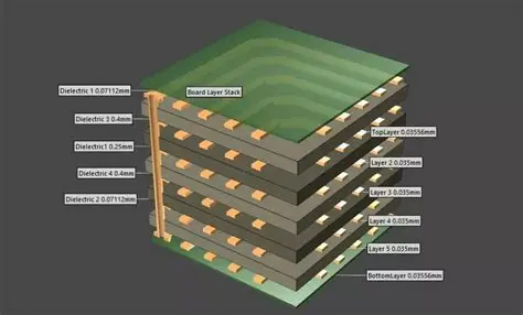
Polyimide PCBs utilize polyimide films as the base dielectric, offering superior properties like glass transition temperatures exceeding 250 degrees Celsius, low thermal expansion, and high tensile strength. These attributes make them ideal for flexible, rigid-flex, and high-reliability rigid boards where standard materials fail under extreme conditions. However, the inherent cost stems from the polyimide substrate itself, which is far more expensive than epoxy-based alternatives due to complex synthesis and limited suppliers. Additional drivers include multilayer stackups, precise copper etching for fine features, and specialized coverlay application over solder mask.
Manufacturing polyimide PCBs involves unique steps like lamination with adhesives, laser drilling for vias, and controlled flexing tests, each adding labor and equipment time. Yield rates can suffer from material sensitivity to moisture and handling, further inflating per-unit expenses. Engineers must identify these factors early to target polyimide PCB material cost reduction effectively. For instance, excessive layer counts or tight bend radii amplify processing difficulties and waste.
Core Technical Principles Behind Polyimide PCB Costs
The primary cost mechanism in polyimide PCBs revolves around material utilization efficiency, where substrate thickness and copper weight directly influence raw material expenses. Thinner polyimides reduce weight and cost but demand precise control to avoid defects like cracking during flexing. Copper foil thickness, typically 1 oz or less for flex applications, balances conductivity with etch yields; heavier foils increase material use without proportional benefits in most designs.
Processing challenges arise from polyimide's chemical resistance, requiring plasma etching or specialized chemicals for vias and patterning, which extend cycle times. Thermal management during lamination prevents delamination, necessitating controlled ovens and pressure profiles. Tolerances for trace widths below 75 microns or spaces under 100 microns escalate inspection needs, as per factory-driven quality checks. Understanding these principles enables targeted polyimide PCB design optimization to minimize waste and rework.
Adhesion between copper and polyimide layers relies on surface treatments, where inadequate bonding leads to peels and scrap. Flex areas introduce warpage risks from asymmetric stackups, demanding balanced designs. These engineering mechanisms highlight why holistic optimization across design and manufacturing phases yields the greatest savings.
Polyimide PCB Design Optimization for Cost Savings
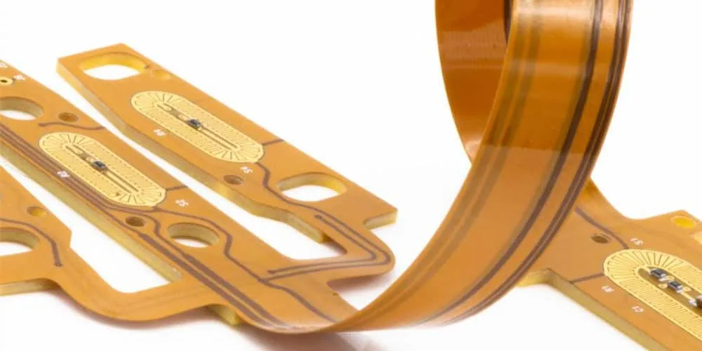
Optimizing polyimide PCB design begins with minimizing the flex area to only essential regions, reducing expensive substrate usage while maintaining functionality. Engineers should standardize polyimide thicknesses, such as 25 or 50 microns, to leverage volume pricing and simplify tooling. Streamlining stackups by combining rigid and flex sections judiciously avoids unnecessary layers; for example, transitioning from multilayer flex to single-layer where signals permit cuts material by up to significant portions without data.
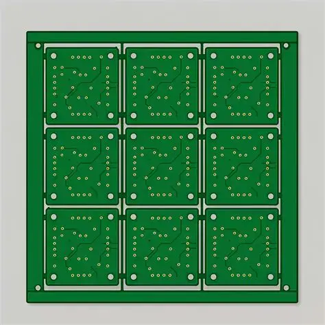
Routing strategies play a pivotal role: grouping traces to shorten lengths reduces copper consumption and improves etch yields. Avoiding blind or buried vias in favor of through-hole types simplifies drilling, especially in polyimide where laser processes add cost. Panelization during design maximizes panel yield, fitting more boards per sheet to amortize setup fees. Incorporating design for manufacturability rules early prevents iterations that delay production.
Coverlay selection impacts both cost and performance; opting for adhesive-based polyimide coverlay over liquid photoimageable alternatives suits high-volume runs with standard outlines. Bend radius optimization per IPC-2223 guidelines prevents stress concentrations, enhancing yield. These polyimide PCB design optimization tactics collectively lower material and processing expenses through efficiency.
Enhancing Polyimide PCB Manufacturing Efficiency
Factory-driven insights emphasize process standardization to boost polyimide PCB manufacturing efficiency. Implementing sequential lamination for rigid-flex builds controls thermal expansion mismatches, reducing warpage and scrap rates. Plasma cleaning before bonding improves adhesion consistency, minimizing defects traceable to poor interfaces.
Yield improvement hinges on moisture control, storing polyimides in dry cabinets to prevent hydrolysis during processing. Automated optical inspection tailored for fine-pitch features catches issues early, avoiding downstream assembly failures. Higher production volumes spread fixed costs like tooling and setups, making bulk orders a cornerstone of cost reduction.
Adhering to IPC-6013 qualification specifications ensures performance without over-engineering, as these outline acceptance criteria for flex boards. Optimizing etch parameters for copper weight uniformity enhances panel utilization. Coverlay lamination under vacuum reduces bubbles, streamlining final profiling. These practices transform manufacturing from a cost center to a value driver.
Advanced Best Practices and Standards Integration
Integrating standards like IPC-2223 for sectional design provides structured guidelines on flex-rigid transitions, preventing common pitfalls like uneven strain distribution. Engineers apply these to specify annular rings and via plating thicknesses that balance reliability with economy. Factory protocols aligned with J-STD-001 for soldering ensure first-pass yields in assembly phases.
Troubleshooting warpage involves symmetric stackups and fixture-controlled cooling post-lamination. For high-reliability apps, selective reinforcement with polyimide stiffeners targets mechanical stress points without full coverage. Data logging process parameters enables continuous refinement, as variations in lamination pressure directly affect impedance control.
Procurement teams benefit from specifying standard copper finishes like ENIG only where needed, defaulting to HASL for cost-sensitive areas. Collaborative design reviews between engineering and manufacturing teams catch optimization opportunities pre-production.
Conclusion
Polyimide PCB material cost reduction, polyimide PCB design optimization, and polyimide PCB manufacturing efficiency form an interconnected framework for substantial savings. By minimizing material use through targeted designs, standardizing processes, and leveraging volume efficiencies, engineers achieve high-performance boards at lower costs. Adherence to key standards ensures quality remains uncompromised. Implementing these strategies requires upfront planning but delivers long-term value in competitive markets. Teams ready to prototype refined designs will see immediate impacts on budgets and timelines.
FAQs
Q1: How can polyimide PCB material cost reduction be achieved without sacrificing thermal performance?
A1: Focus on thinner standard polyimide films and optimized copper weights suited to current demands. Limit flex areas to functional necessities and panelize designs for better yield. Factory processes like controlled lamination per IPC-6013 maintain integrity while cutting waste. This approach balances expense with reliability for electric engineers.
Q2: What are essential polyimide PCB design optimization steps for manufacturing efficiency?
A2: Standardize layer counts, trace routings, and bend radii following IPC-2223 guidelines to simplify etching and assembly. Use through-vias over lasers where possible and symmetric stackups to prevent warpage. Early DFM reviews ensure compatibility, reducing iterations and boosting throughput.
Q3: Why does polyimide PCB manufacturing efficiency vary, and how to improve it?
A3: Variations stem from material handling sensitivity and process controls; improve via dry storage, plasma treatments, and automated inspections. Higher volumes amortize setups, while yield-focused parameters like etch uniformity lower scrap. Standards compliance streamlines qualification for consistent output.
Q4: When should engineers prioritize polyimide over cheaper substrates in cost-sensitive projects?
A4: Reserve polyimide for applications needing high flexure cycles or temperatures beyond FR-4 limits, optimizing elsewhere via minimal layers and standard features. Cost-benefit analysis weighs material premiums against lifecycle savings from reliability.
References
IPC-2223 — Sectional Design Standard for Flexible Printed Boards. IPC.
IPC-6013 — Qualification and Performance Specification for Flexible Printed Boards. IPC.
J-STD-001 — Requirements for Soldered Electrical and Electronic Assemblies. IPC, J-STD.





