 ALLPCB


Introduction
Component placement plays a critical role in determining the testability of printed circuit boards during manufacturing and assembly phases. Engineers must consider how the positioning of components affects access for test probes, fixtures, and automated equipment to ensure reliable fault detection. Poorly optimized layouts can lead to shadowed nodes, increased test times, and higher costs associated with custom fixtures. By focusing on component placement for testability from the initial design stage, teams can streamline production processes and improve overall yield. This article delves into the engineering principles, best practices, and strategies for enhancing test access through thoughtful layout decisions. Understanding these factors helps electric engineers create robust designs that balance functionality with manufacturability.
Understanding Component Placement for Testability
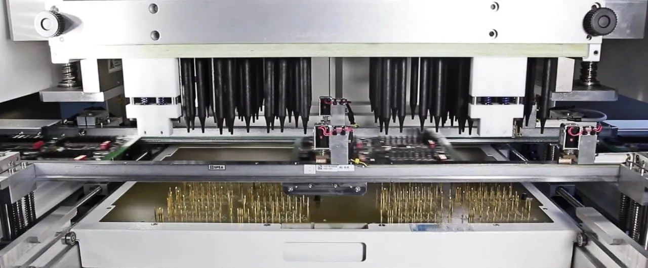
Component placement for testability refers to the strategic arrangement of electronic parts on a PCB to facilitate various testing methods, such as in-circuit testing, flying probe testing, and boundary scan. Testability encompasses the ability to verify electrical connectivity, component functionality, and assembly integrity without excessive complexity. Key aspects include ensuring sufficient clearance around test points, avoiding component overlap that blocks probe access, and grouping related signals for efficient node isolation. In high-density boards, where space constraints challenge traditional testing approaches, this optimization becomes even more essential. Engineers evaluate placement against test strategy requirements early to prevent downstream rework. Ultimately, effective component placement for testability reduces diagnostic ambiguity and supports faster time-to-market.
Why Optimizing Component Layout Matters for Testability
Optimizing component layout directly impacts the efficiency and cost of PCB testing in production environments. Inaccessible or densely packed areas complicate fixture design, often requiring specialized probes or extended programming time. This can escalate test fixture costs, as custom adaptations become necessary for shadowed vias or closely spaced pins. Moreover, poor layouts increase the risk of false failures due to probe misalignment or mechanical stress on components. Industry practices emphasize layout optimization to align with common test platforms, ensuring compatibility across facilities. By prioritizing test access during placement, designers minimize these challenges and enhance fault coverage.
Improved test access through component placement also correlates with higher assembly yields. When probes can reliably contact nets without interference, test throughput rises, reducing cycle times. This approach aligns with broader design for manufacturability goals, where testability serves as a key metric. Electric engineers benefit from layouts that support multiple test methodologies, providing flexibility for evolving production needs. In summary, strategic optimization not only safeguards quality but also controls operational expenses.
Technical Principles Governing Component Placement and Testability
The foundational principles of component placement for testability revolve around probe accessibility, nodal density, and mechanical stability. Probes require a minimum clearance zone around each test point, typically dictated by fixture pin diameters and board tolerances. Components positioned too closely can create guard bands that shield underlying nets, necessitating angled or longer probes which raise fixture complexity. Electrical principles, such as minimizing capacitive coupling between adjacent test points, further guide placement to avoid measurement errors during high-impedance tests. Thermal considerations during testing also influence layout, as clustered power components may generate hotspots that affect probe reliability.
Guard banding and pitch requirements form the core of these principles. Standard probe spacing demands at least 100 mil separation between accessible points to accommodate common bed-of-nails fixtures. Vias and test pads must remain unobstructed on the primary test side, often the bottom, to simplify fixture construction. IPC-2221 provides guidelines for component spacing and routing that indirectly support testability by promoting orderly layouts. Overlapping component shadows reduce effective test coverage, forcing reliance on functional testing which is less precise for opens and shorts. Engineers apply these principles iteratively during layout reviews to balance density with accessibility.
Signal integrity principles extend to testability, as high-speed nets demand controlled impedance paths unhindered by test hardware. Placement that clusters analog and digital sections separately aids in isolating noise during tests. Fixture pressure distribution must avoid board flexure, so heavy components like connectors benefit from edge placement to stabilize probing. These mechanisms ensure that component placement supports both structural and electrical test objectives without compromise.
DFT Guidelines for Component Placement
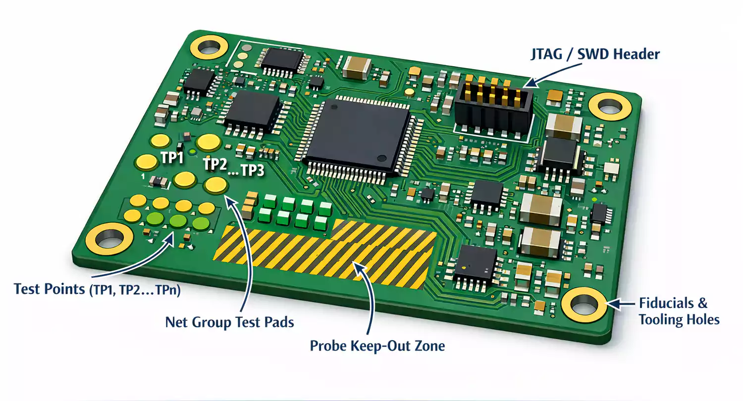
Design for testability (DFT) guidelines for component placement emphasize proactive measures to embed test features into the layout. Dedicate test points to critical nets, positioning them away from component leads and solder masks. Place these pads on the non-component side where possible, ensuring a flat, probe-friendly surface. Group test points logically by functional blocks to streamline fixture wiring and reduce crosstalk. Avoid placing fine-pitch components directly over high-priority test nets, as solder joints can obstruct access post-assembly.
Adherence to DFT involves standardizing pad geometries for universal probe compatibility. Rectangular or oblong test pads offer better contact reliability than circular ones under varying pressures. Maintain consistent orientation for polarized components to prevent test program errors. J-STD-001 outlines requirements for soldered connections that influence post-assembly test access, stressing clean profiles free of bridges. Integrate boundary scan chains early, routing JTAG pins to board edges for easy connector access. These guidelines form a checklist for reviewers, ensuring comprehensive coverage.
Fixture minimization through DFT targets reducing custom tooling by leveraging standard grids. Orient components to align test points on a 0.1-inch matrix, common in industry fixtures. Limit via-in-pad usage under components unless testable via flying probe. IPC-A-610 criteria for acceptability reinforce these by specifying visual and electrical verification points. By following DFT guidelines for component placement, designs achieve higher fault detection rates with minimal adaptation.
Best Practices for Optimizing Component Layout
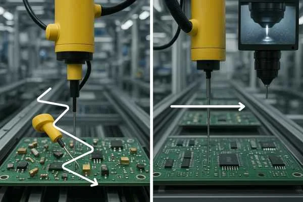
Optimizing component layout begins with partitioning the board into testable zones during schematic capture. Place high-priority test nets near edges or open areas, reserving central regions for dense logic. Sequence placement by signal flow: start with connectors and power devices, then populate ICs, followed by passives. This hierarchy exposes key nodes early. Simulate probe access using design rule checks customized for test clearances. Iterate layouts with manufacturing input to validate fixture feasibility.
To minimize test fixture cost, standardize on fewer unique probe lengths and angles. Flat-top components like resistors should face the test side, providing landmarks for alignment. Avoid tall profiles over test pads, opting for low-profile alternatives where function allows. Route traces to expose inner layer nets via dedicated vias, enhancing access without extra pads. Collaborative reviews between design and test teams refine these practices, catching issues pre-gerber.
Improving test access extends to multi-layer boards, where blind vias aid surface probing. Cluster bypass capacitors near ICs but offset from pins to prevent shadowing. For mixed-technology assemblies, segregate through-hole parts to fixture edges, easing nail placement. These practices, grounded in engineering logic, yield layouts resilient to production variances.
Strategies to Minimize Test Fixture Cost Through Placement
Minimizing test fixture cost hinges on component placement that favors off-the-shelf tooling. Design for 5 mil probe tolerance by enforcing generous keep-out zones around nets. Limit test point count to essentials via netlist analysis, prioritizing opens/shorts coverage. Position components to allow universal fixture bases, reducing machining for custom plates. Edge connectors for power and ground simplify fixturing, cutting wiring expenses.
Cost savings accrue from reduced programming and debug time enabled by accessible layouts. Standardize test grid alignment across product families for reusable fixtures. Avoid polarities that demand fixture rotation, standardizing top-side probing. These strategies compound, lowering per-unit test overhead significantly.
Case Study: Enhancing Testability in a High-Density Design
Consider a multilayer control board with mixed signal ICs and fine-pitch BGAs. Initial placement clustered components densely, shadowing 30% of nets and requiring a complex flying probe setup. Redesign applied DFT guidelines, relocating passives and adding edge test pads per IPC-2221 spacing rules. Test access improved, allowing bed-of-nails fixturing with standard pins. Fixture cost dropped, and fault detection rose due to clearer nodal isolation. This logical restructuring demonstrated the tangible benefits of optimized component layout.
Conclusion
Strategic component placement profoundly influences PCB testability, affecting everything from probe access to fixture economics. By integrating DFT guidelines early, engineers optimize layouts for reliable, cost-effective testing. Key practices like clearance enforcement, test point dedication, and zonal partitioning ensure robust designs. Adhering to standards such as IPC-2221 and J-STD-001 reinforces these efforts. Electric engineers who prioritize component placement for testability gain superior manufacturability and quality outcomes. Implementing these principles elevates design excellence across projects.
FAQs
Q1: What are the primary DFT guidelines for component placement in PCB design?
A1: DFT guidelines for component placement stress dedicating test pads to every critical net, maintaining 100 mil probe spacing, and avoiding component overhangs on test points. Place high-density areas away from primary probe sides, using the bottom for access. Group signals by function to simplify fixtures. These steps, aligned with J-STD-001 soldered joint requirements, enhance fault isolation and reduce test complexity. Follow IPC-2221 for baseline spacing to ensure compatibility.
Q2: How does optimizing component layout minimize test fixture cost?
A2: Optimizing component layout minimizes test fixture cost by standardizing probe access on common grids, reducing custom machining needs. Exposed test points eliminate special angled pins, while edge-placed connectors cut wiring. Logical grouping lowers point counts, shortening programming. This approach supports reusable fixtures, directly impacting expenses. Electric engineers see savings through higher throughput and fewer adaptations.
Q3: Why is improving test access crucial in component placement for testability?
A3: Improving test access in component placement for testability prevents shadowed nodes that cause incomplete coverage or false passes. Clear paths for probes ensure accurate opens, shorts, and parametric checks. It supports scalable testing from ICT to functional methods. Densely packed boards risk fixture damage or board stress without it. Prioritizing access upholds quality in high-volume production.
Q4: What role do industry standards play in PCB component placement for testability?
A4: Industry standards like IPC-A-610 and IPC-2221 guide component placement for testability by defining spacing, orientation, and acceptability criteria. They promote layouts compatible with standard test equipment. J-STD-001 ensures assembly features support probing. These references provide a framework for consistent, reliable designs without custom deviations.
References
IPC-2221G — Generic Standard on Printed Board Design. IPC, 2012
J-STD-001H — Requirements for Soldered Electrical and Electronic Assemblies. IPC, 2018
IPC-A-610H — Acceptability of Electronic Assemblies. IPC, 2019


