 ALLPCB


Introduction
In modern PCB design, vias serve as critical interconnects between layers, but unfilled vias can introduce reliability issues such as solder wicking, contamination, or thermal stress during assembly and operation. Selecting the optimal PCB via fill material addresses these challenges by enhancing mechanical stability, electrical performance, and thermal management. This decision directly impacts the overall reliability of the PCB design, particularly in high-density interconnects or applications with stringent environmental requirements. Engineers must evaluate material properties against specific design goals to ensure compliance with performance standards. PCB via fill material selection involves balancing conductivity needs, cost, and process compatibility. Ultimately, the right choice supports robust, long-term functionality in diverse applications.
What Are Via Fill Materials and Why Do They Matter?
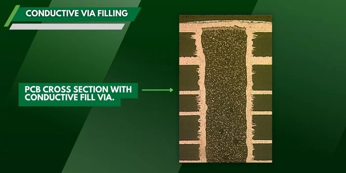
Via fill materials are substances used to completely or partially occupy the drilled hole in a via after plating, transforming an open structure into a solid one. This process, known as via filling or plugging, eliminates voids that could trap contaminants or cause failures during reflow soldering. In high-reliability designs, filled vias prevent issues like pad cratering or delamination under thermal cycling. The importance escalates in dense boards where components mount directly over vias, requiring a planar surface for uniform solder joints. According to IPC-4761, various via protection methods, including filling, define benchmarks for coverage and integrity. Proper via fill contributes to reliable PCB design by mitigating risks associated with mechanical shock, vibration, and humidity exposure.
Unfilled vias expose the board to solder migration during assembly, potentially shorting adjacent traces or weakening joints. Filled vias, conversely, provide structural reinforcement, distributing stress more evenly across layers. This is particularly vital in multilayer boards where via aspect ratios exceed 1:1, increasing plating challenges. Material selection influences signal integrity by reducing impedance discontinuities in high-speed designs. Thermal dissipation improves with conductive fills, preventing hotspots in power planes. Overall, via fill enhances manufacturability and field performance, aligning with engineering goals for durability.
Types of Via Fill Materials: Conductive vs. Non-Conductive
Via fill materials divide primarily into conductive and non-conductive categories, each suited to distinct electrical and thermal demands. Conductive fills, such as copper or silver-loaded epoxy, maintain electrical continuity through the via while offering superior heat transfer. These materials exhibit thermal conductivities significantly higher than non-conductive options, making them ideal for thermal vias under power components. Non-conductive fills, typically epoxy resins, prioritize insulation and surface planarity without adding unintended paths. The choice hinges on whether the via functions solely for interlayer connection or requires additional dissipation capabilities.
Conductive vs. non-conductive fill material selection depends on application specifics. Conductive types excel in high-current paths, where low resistance ensures minimal voltage drop. However, they demand precise process control to avoid voids or cracking during curing. Non-conductive fills simplify assembly by blocking solder entry, crucial for BGA footprints. Both categories must match the PCB's coefficient of thermal expansion to prevent cracking under temperature swings.
Epoxy vs. Copper Fill Material: A Detailed Comparison
Epoxy fills, available in both conductive and non-conductive forms, provide cost-effective solutions with good adhesion to copper plating. Non-conductive epoxy offers low viscosity for complete void-free filling, essential for microvias under 0.15 mm diameter. Conductive epoxy incorporates metal particles for moderate conductivity, bridging the gap between pure insulation and full metallization. Copper fill, achieved via electroplating after initial resin plug, delivers the highest thermal and electrical performance, akin to solid copper traces. Epoxy vs. copper fill material trade-offs center on cost, with copper processes adding steps like additional plating cycles.
Copper-filled vias achieve near-bulk copper properties, with thermal conductivity around 400 W/mK, far surpassing epoxy's 1-3 W/mK range. This makes copper preferable for RF or power applications demanding low inductance. Epoxy, however, cures faster and tolerates higher aspect ratios without dimpling. Surface finish after filling requires capping plating per IPC-6012 requirements, ensuring flatness within specified tolerances. Engineers weigh these against board complexity; epoxy suits prototype volumes, while copper fits production high-rel designs. Compatibility with subsequent processes, like ENIG finish, further guides the decision.
Key Factors Influencing PCB Via Fill Material Selection
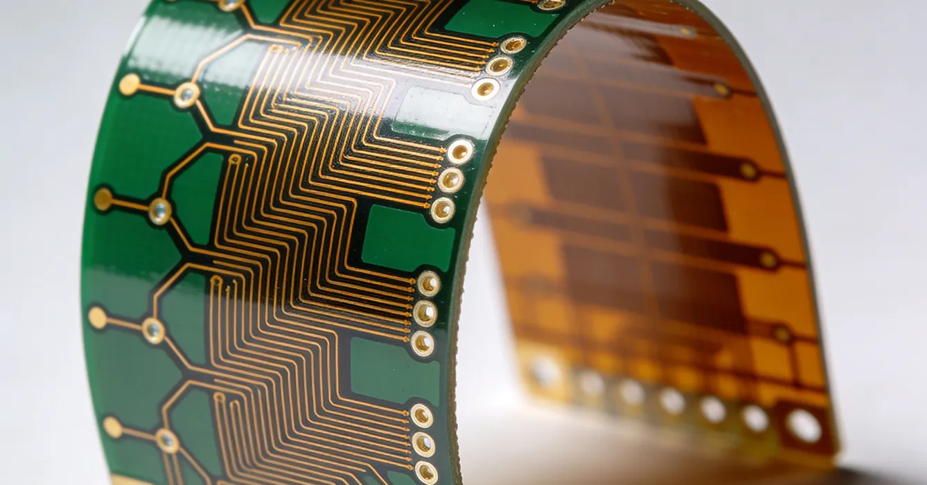
Thermal management stands as a primary factor, where conductive materials dissipate heat from inner layers to surfaces efficiently. In designs with dense power routing, unfilled vias act as insulators, exacerbating hotspots. Electrical requirements dictate conductive fills for signal vias needing low resistance, while non-conductive suffices for blind or buried types. Mechanical reliability involves matching CTE between fill, laminate, and copper to avoid fatigue cracks during thermal cycling. Flexible PCBs demand materials with elasticity to accommodate bending without fracturing the fill.
Process compatibility influences selection, as high-viscosity fills risk incomplete penetration in deep vias. Cost escalates with conductive options due to material and plating expenses, impacting high-volume production. Environmental factors, such as operating temperature range, require fills stable beyond 125°C without outgassing. For reliable PCB design, simulate via performance using finite element analysis to predict stress concentrations. Aspect ratio limits, typically under 1:1 for reliable filling, guide via sizing early in layout.
Material for flexible PCBs prioritizes low-modulus epoxies compatible with polyimide substrates. These maintain flexibility while sealing vias against moisture ingress during flexing. Conductive fills in flex circuits risk cracking under repeated bends, favoring non-conductive for dynamic regions. Static zones tolerate copper for better performance. Selection ensures the fill withstands millions of cycles without degradation.
Best Practices for Implementing Via Fills in PCB Design
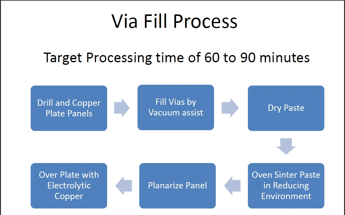
Specify via fill requirements in fabrication notes, detailing material type and acceptance criteria like void percentage under 10%. Design vias with diameters at least 0.2 mm for standard fills, scaling down for HDI with laser drilling. Place thermal vias in arrays under heat sources, filled conductively to maximize spread. Verify planarity post-fill via profilometry, targeting dimple depths below 0.076 mm as per standards. For epoxy, use vacuum-assisted dispensing to eliminate air pockets, enhancing reliability.
Integrate via-in-pad processes by tenting soldermask before filling, preventing resin bleed. Test filled prototypes with thermal cycling per IPC-6012 to validate integrity. Collaborate with fabricators on fill methods like screen printing for large panels or inkjet for precision. Avoid overfilling to prevent protrusion affecting component coplanarity. These practices yield reliable PCB design across classes 2 and 3.
In high-density boards, prioritize non-conductive fills for non-critical vias to control costs without compromising function. Conductive fills reserve for bottlenecks like ground returns. Document fill types in stackup drawings for traceability. Post-assembly X-ray inspection confirms fill completeness.
Special Considerations for Flexible and High-Reliability Applications
Flexible PCBs require fills with elongation exceeding 50% to endure repeated flexing without delamination. Non-conductive epoxies formulated for polyimide bonding prevent moisture wicking along interfaces. In rigid-flex hybrids, transition zones use hybrid fills to bridge material differences. High-reliability sectors, like aerospace, mandate conductive copper fills per IPC-4761 Type VI for mission-critical thermal paths.
Troubleshoot common issues like fill cracking by adjusting cure profiles or selecting lower-CTE materials. Warpage minimization involves symmetric stacking with balanced fills. These insights ensure optimal performance in demanding environments.
Conclusion
Choosing the optimal via fill material hinges on a systematic evaluation of thermal, electrical, mechanical, and cost factors tailored to the PCB's application. Conductive options like copper excel in performance-critical scenarios, while epoxy provides versatile, economical alternatives. Adhering to standards such as IPC-4761 and IPC-6012 guarantees compliance and reliability. For flexible PCBs, prioritize compatible, elastic materials to maintain integrity under deformation. Implementing best practices from design through verification fosters robust, high-yield production. Ultimately, informed PCB via fill material selection elevates the entire design to dependable operation.
FAQs
Q1: What factors should electric engineers consider in PCB via fill material selection?
A1: Engineers must assess thermal conductivity, CTE matching, and electrical needs alongside cost and process compatibility. Conductive fills suit high-power vias, while non-conductive epoxy prevents solder issues in dense layouts. Standards like IPC-4761 guide protection types for reliable PCB design. Proper selection minimizes failures in assembly and field use.
Q2: How does epoxy vs. copper fill material impact thermal performance?
A2: Copper fill offers superior thermal conductivity for efficient heat spreading in power applications, reducing hotspots. Epoxy, even conductive variants, provides moderate dissipation suitable for signal vias. Copper processes ensure bulk-like properties but increase complexity. Choice aligns with operating temperatures for reliable PCB design. Non-conductive epoxy prioritizes planarity over heat transfer.
Q3: What is the best material for flexible PCBs in via filling?
A3: Non-conductive epoxy with high flexibility and polyimide compatibility serves as the primary choice for dynamic regions, preventing cracks during bending. Conductive options limit to static areas for thermal needs. Low-modulus fills maintain seal integrity against fatigue. This supports reliable PCB design in wearable or aerospace flex circuits.
Q4: When to use conductive vs. non-conductive fill material?
A4: Use conductive fills for vias requiring electrical continuity or heat dissipation, like thermal vias under ICs. Non-conductive suits insulating interlayer connections or BGA sites to block solder wicking. Evaluate based on signal speed and power density for optimal performance. IPC-6012 criteria ensure plating and fill quality in reliable PCB design.
References
IPC-4761 — Via Protection and Covering Requirements for Printed Boards. IPC, 2007
IPC-6012E — Qualification and Performance Specification for Rigid Printed Boards. IPC, 2017
IPC-6012DS — Qualification and Performance Specification for High Density Interconnect (HDI) Printed Boards. IPC, 2016


