 ALLPCB


Introduction
In high-frequency PCB design, maintaining signal integrity is crucial as data rates continue to rise and board densities increase. Vias, essential for interlayer connections, often introduce discontinuities that degrade performance through reflections and impedance mismatches. Unfilled through-hole vias create stubs that act as open-ended transmission lines, leading to significant signal reflections at frequencies above a few gigahertz. Via filling addresses these challenges by eliminating the stub, providing a more uniform signal path and better impedance control with vias. This approach is particularly vital for applications demanding low bit error rates and high bandwidth. By understanding the impact of via filling on signal integrity, engineers can optimize PCB layouts for superior performance.
Engineers working on multilayer boards recognize that via stub effects become pronounced when stub lengths approach quarter-wavelength dimensions at operating frequencies. Filling the via with conductive or non-conductive materials transforms it into a solid interconnect, minimizing these effects. This technique supports reducing signal reflections without relying solely on backdrilling, which may not suit all designs. The result is improved return loss and insertion loss characteristics across the signal path. As PCB complexity grows, integrating via filling into the design flow ensures compliance with performance requirements from the outset.
Understanding Via Stub Effects in High-Frequency PCB Design
Via stubs occur in through-hole vias where the unused portion beyond the innermost connected layer extends as an unterminated line. This stub introduces an impedance discontinuity because the signal encounters an abrupt open circuit, causing partial reflection back toward the source. The reflection coefficient depends on the mismatch between the trace impedance and the effective impedance of the stub, typically resulting in increased return loss. At high frequencies, these reflections superimpose with the original signal, leading to eye diagram closure and potential data errors. Engineers must model these effects using transmission line theory to predict behavior accurately.
The resonant frequency of a via stub aligns with its electrical length equaling a quarter wavelength, where it behaves like a parallel resonant circuit, maximizing energy storage and reflection. For a typical 1.6 mm thick board with dielectric constant around 4, this resonance might fall in the 3 to 5 GHz range, critical for many modern interfaces. Signal integrity via filling targets this exact issue by removing the resonant element entirely. Without mitigation, multiple vias compound the problem through crosstalk and cumulative jitter. High-frequency PCB design thus demands proactive stub management to preserve signal quality.
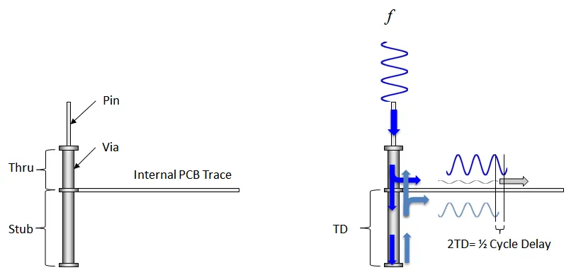
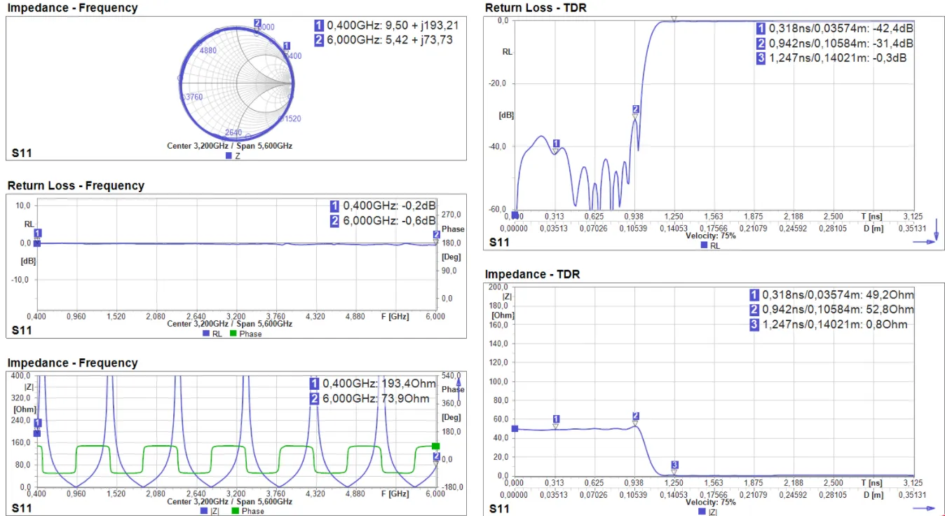
Quantifying stub impact involves time-domain reflectometry (TDR) measurements, where a step signal reveals impedance steps at via transitions. Uncontrolled stubs show pronounced ringing in time-domain simulations, correlating to frequency-domain notches in S-parameters. Reducing signal reflections requires either shortening the stub via blind or buried vias or filling it completely. Each method trades off fabrication complexity against performance gains. In dense designs, via filling offers a compact solution without altering layer stackup significantly.
The Role of Via Filling in Signal Integrity
Via filling involves completely filling the plated through-hole with a material, either conductive like copper or non-conductive like epoxy resin, to eliminate the hollow core and stub. This process creates a seamless vertical interconnect that mimics a continuous conductor, vastly improving impedance control with vias. Conductive filling maintains low resistance and supports current carrying, while non-conductive variants suffice for signal paths where thermal or mechanical stability is prioritized. The filled via reduces parasitic inductance and capacitance variations, leading to smoother TDR profiles.
According to IPC-4761, various via protection and filling configurations are classified to guide selection based on reliability needs. This standard outlines requirements for covered, filled, and plugged vias, ensuring process control during fabrication. Signal integrity benefits emerge because the filled structure prevents air gaps that could trap contaminants or cause plating voids. In practice, filled vias enable tighter routing grids and via-in-pad designs, common in high-density interconnects. Engineers appreciate how this enhances overall board reliability under thermal cycling.
Via filling directly counters via stub effects by presenting a uniform dielectric and conductor profile along the signal path. Reflections diminish as there is no distal open end to reflect energy back. This is especially effective for differential pairs crossing layers, where pair skew from asymmetric stubs is eliminated. Fabrication processes like electroplated copper filling achieve high fill densities without voids, verified through cross-section analysis. The technique integrates well into standard multilayer flows, making it accessible for production-scale designs.
Mechanisms for Reducing Signal Reflections Through Via Filling
Reflections in vias stem primarily from the open stub acting as a high-impedance reflector, with reflection magnitude approaching 100% at resonance. Filling the via shorts the stub electrically in conductive cases or dielectrically loads it in non-conductive fills, detuning the resonance and damping the response. Impedance control with vias improves as the effective diameter and surrounding field distribution align better with adjacent traces. Simulations confirm that filled vias exhibit return loss exceeding 20 dB up to higher frequencies compared to unfilled counterparts, though exact figures depend on stackup.
The inductance of an unfilled via is higher due to the larger loop area around the plating barrel, exacerbating voltage droop and ringing. Conductive filling minimizes this by providing a solid core, reducing loop inductance by factors related to fill conductivity. Capacitance to adjacent planes stabilizes further with controlled fill materials matching board dielectric constants. These changes collectively broaden usable bandwidth, critical for high-frequency PCB design. Reducing signal reflections thus involves holistic via optimization, not isolated fixes.
In frequency-domain terms, S11 parameters show nulls from stub resonances shifting or vanishing post-filling. Eye height and width metrics improve, with jitter components tied to reflections suppressed. Non-conductive fills introduce minor propagation delay but negligible loss for most signals. Engineers can verify via fill efficacy through vector network analyzer sweeps pre- and post-fabrication. This data-driven approach ensures design margins hold across process variations.
Best Practices for Via Filling in High-Frequency Designs
Select via filling when stub lengths exceed one-twentieth of the minimum wavelength, typically signaling potential integrity risks. Prioritize conductive filling for power or high-current signals, reserving non-conductive for pure interconnects to balance cost. Design via diameters to fabrication capabilities, ensuring anti-pad clearances support plating overflow without bridging. IPC-6012E specifies qualification tests for filled vias, including thermal shock and electrical continuity to validate performance. Simulate early with 3D field solvers to predict fill impacts on nearby traces.
Integrate via filling into the layer stackup planning, coordinating with fabricators for fill type and cap plating. For impedance control with vias in controlled stacks, adjust trace widths adjacent to vias to compensate for any residual discontinuity. Avoid over-filling processes that induce stress cracks; controlled electroforming yields uniform results. In HDI boards, filled microvias enable fanout from fine-pitch components without stub penalties. Regular process audits maintain consistency across production lots.
Backdrilling offers an alternative for longer stubs but increases drill steps and potential debris issues, making filling preferable for dense, thin boards. Combine with ground via stitching around signal vias to further shield and return currents. Document fill requirements in fabrication drawings clearly, specifying IPC compliance. These practices ensure signal integrity via filling delivers measurable gains in prototype and volume production.
Advanced Design Considerations for Optimized Performance
In multilayer high-speed boards, cluster multiple filled vias for power distribution to handle current without hotspots. Material selection for fills should consider CTE matching to copper and laminate, preventing reliability failures under reflow. For RF signals, prioritize low-loss fills to minimize tan delta contributions. Via fence configurations with filled vias enhance isolation between adjacent signals. Engineers benefit from iterative PDN analysis incorporating filled via models for voltage integrity.
Planar equalization near filled vias can fine-tune insertion loss equalization if needed. Stackup symmetry aids in maintaining consistent via performance across layers. Fabrication yields improve with panel-level fill processes over sequential board filling. These considerations position via filling as a cornerstone of robust high-frequency PCB design.
Conclusion
Via filling profoundly enhances signal integrity by eliminating stub-induced reflections and stabilizing impedance profiles. This technique proves indispensable for modern high-frequency PCB design, enabling reliable performance at elevated data rates. By adhering to standards like IPC-4761 and IPC-6012E, engineers achieve predictable results without excessive design iterations. Implementing best practices ensures via filling contributes to overall board success, from simulation to deployment. Prioritizing this in early design stages minimizes risks and maximizes margins.
FAQs
Q1: What is signal integrity via filling and when should it be used?
A1: Signal integrity via filling refers to completely filling through-hole vias with conductive or non-conductive materials to eliminate stubs that cause reflections. Use it in high-frequency PCB design when operating frequencies exceed stub quarter-wavelength resonances, typically above 2-3 GHz depending on board thickness. This maintains impedance control with vias, reduces return loss, and supports dense routing. Fabricators classify options per IPC-4761 for reliability.
Q2: How does via filling help in reducing signal reflections?
A2: Via filling removes the open-ended stub that reflects signals back due to impedance mismatch, creating a uniform transmission path. Reflections diminish as parasitic inductance and capacitance even out, improving TDR responses and eye diagrams. This is critical for via stub effects in multilayer boards. Conductive fills provide the best electrical continuity, while non-conductive suits lighter duties. Simulations validate gains before fabrication.
Q3: What are best practices for impedance control with vias using filling?
A3: Optimize via size and anti-pad to match trace impedance, selecting fill types per signal needs. Simulate 3D models incorporating fill properties for accurate predictions. Reference IPC-6012E for qualification to ensure plating integrity. Place ground returns near signal vias and verify with S-parameter tests. This approach minimizes discontinuities in high-frequency PCB design effectively.
Q4: Can via filling replace backdrilling for high-speed signals?
A4: Via filling often serves as a superior alternative to backdrilling by fully eliminating stubs without additional drill steps, ideal for thin or dense boards. It offers better mechanical stability and supports via-in-pad layouts. However, backdrilling suits thicker stacks where fill costs rise. Choose based on stackup and frequency; both reduce via stub effects for signal integrity.
References
IPC-4761 — Via Protection and Covering Requirements for Printed Boards. IPC, 2007
IPC-6012E — Qualification and Performance Specification for Rigid Printed Boards. IPC, 2015
IPC-2221G — Generic Standard on Printed Board Design. IPC, 2012


