 ALLPCB


When it comes to designing RF PCBs (Radio Frequency Printed Circuit Boards), size plays a critical role in determining performance. For engineers and designers working on RF applications, understanding how PCB size affects signal integrity, antenna placement, impedance control, and overall efficiency is essential. In this comprehensive guide, we’ll explore the impact of PCB size for RF applications, key considerations in RF PCB design, and actionable tips to optimize performance while minimizing signal loss.
Whether you’re working on wireless communication devices, IoT hardware, or 5G technology, the size of your RF PCB can make or break your project. Smaller boards may save space but can introduce challenges like signal interference, while larger boards might improve performance but increase costs. Let’s dive into the details of how size influences RF PCB design and what you can do to strike the right balance.
Why PCB Size Matters in RF Applications
In RF PCB design, size isn’t just about fitting components into a compact space. The dimensions of the board directly impact how signals travel, how components interact, and how efficiently the system operates. RF signals, which often operate in the megahertz (MHz) to gigahertz (GHz) range, are highly sensitive to physical layout. Even a small change in board size can lead to significant differences in performance due to factors like signal loss and impedance mismatches.
For instance, a PCB that’s too small may crowd components, leading to crosstalk or electromagnetic interference (EMI). On the other hand, a board that’s too large might introduce longer signal paths, increasing the risk of signal degradation. Finding the optimal PCB size for RF applications requires balancing space constraints with performance needs.
Key Factors in RF PCB Design: How Size Influences Performance
Let’s break down the specific ways that PCB size impacts performance in RF applications. Each of these factors is interconnected, and understanding them will help you make informed decisions during the design process.
1. Signal Loss and Trace Length
Signal loss is a major concern in RF PCB design, and the size of the board directly affects it. Longer traces, often necessary on larger boards, can lead to higher signal attenuation, especially at high frequencies. For example, at 2.4 GHz (a common frequency for Wi-Fi and Bluetooth), a signal traveling along a trace can lose strength due to dielectric losses in the PCB material and resistance in the copper traces. A general rule of thumb is that signal loss increases by approximately 0.1 dB per inch of trace length on standard FR-4 material at 1 GHz.
On smaller boards, traces are shorter, which can reduce signal loss. However, cramming components into a tight space can lead to unwanted coupling between traces, increasing the risk of interference. To mitigate this, designers must carefully plan trace routing and consider using high-frequency laminates with lower dielectric constants (Dk) to minimize losses, regardless of board size.
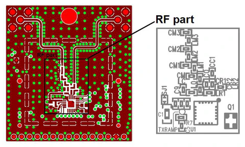
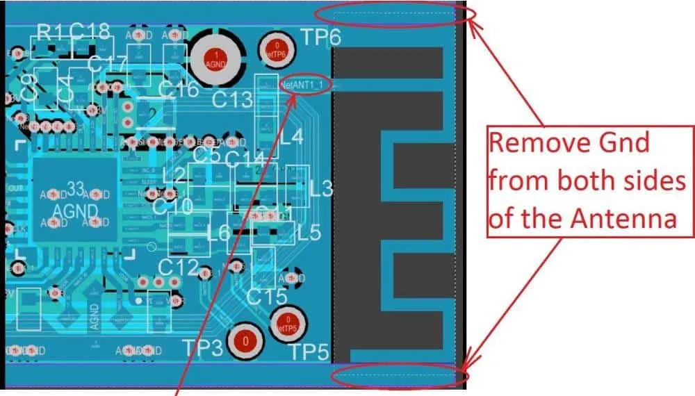
2. Antenna Placement and Efficiency
Antenna placement is another critical aspect of RF PCB design where size plays a significant role. Antennas need adequate space and isolation from other components to function effectively. On a small PCB, placing an antenna too close to other elements like power supplies or digital circuits can cause interference, reducing the antenna’s efficiency and range.
For optimal performance, antennas should ideally be placed at the edge of the board with a clear ground plane beneath them. According to design guidelines for 2.4 GHz applications, a keep-out area of at least 10 mm around the antenna is recommended to avoid interference. Larger boards offer more flexibility for proper antenna placement, but if space is limited, consider using external antennas or carefully designing the layout to maintain isolation.
3. Impedance Control in RF PCBs
Impedance control is vital for ensuring that RF signals travel without reflection or loss of power. In RF PCB design, traces must be designed to match the characteristic impedance of the system, often 50 ohms for most RF applications. The size of the PCB can impact impedance control because it influences trace width, spacing, and the ability to maintain consistent dielectric thickness.
On smaller boards, achieving precise impedance matching can be challenging due to limited space for wider traces or proper spacing. For example, a 50-ohm microstrip trace on a standard 1.6 mm FR-4 board requires a width of about 2.9 mm, which may not fit on a compact design. Larger boards provide more room to adjust trace geometries and incorporate ground planes, making impedance control easier. To address this on smaller boards, consider using thinner substrates or high-frequency materials with lower Dk values to reduce trace widths while maintaining impedance.
4. Ground Plane Design and EMI
A solid and continuous ground plane is essential in RF PCB design to minimize noise and provide a stable reference for signals. The size of the PCB affects how effectively you can implement a ground plane. On larger boards, there’s more area to create a robust ground plane, which helps in reducing EMI and improving signal integrity.
On smaller boards, the ground plane may be fragmented due to space constraints, leading to potential “ground loops” or areas where signals can couple with noise. To combat this, designers should prioritize a dedicated ground layer in the PCB stack-up, even on compact designs, and use vias to connect ground planes across layers for consistency.
Balancing PCB Size with Performance: Practical Tips for RF Applications
Now that we’ve covered the key ways size impacts RF PCB performance, let’s look at some actionable strategies to optimize your design. These tips are tailored for engineers working on RF applications and aim to help you achieve the best results, regardless of board size constraints.
1. Optimize Component Placement
Start by placing critical components like RF transceivers and antennas first. Ensure that high-frequency signal paths are as short as possible to minimize signal loss. Group related components together to reduce trace lengths, but maintain adequate spacing to avoid crosstalk. For compact designs, consider using surface-mount components with smaller footprints to save space without sacrificing performance.
2. Choose the Right Materials
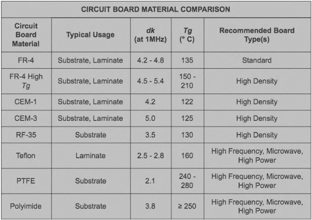
The choice of PCB material is crucial in RF design, especially when size is a limiting factor. Standard FR-4 materials may work for lower frequencies (below 1 GHz), but for higher frequencies, consider laminates with low dielectric constants (Dk around 2.2 to 3.5) and low dissipation factors (Df below 0.002). These materials help reduce signal loss and allow for narrower traces, which is beneficial on smaller boards.
3. Use Simulation Tools
Before finalizing your RF PCB design, use simulation software to model signal behavior and impedance matching. Tools can help you predict how board size and layout affect performance, allowing you to make adjustments early in the design process. For example, simulating a 50-ohm trace at 5 GHz can reveal potential mismatches caused by board dimensions or material properties, saving time and cost during prototyping.
4. Prioritize Stack-Up Design
A well-planned PCB stack-up is essential for RF performance, especially on smaller boards. Use a multi-layer design if possible, dedicating layers to ground planes and power distribution. For a 4-layer board, a common configuration is signal-ground-power-signal, which helps isolate RF signals from noise. On larger boards, additional layers can further improve isolation and routing flexibility.
5. Test and Iterate
Finally, always test your RF PCB design under real-world conditions. Use network analyzers to measure signal loss and impedance, and adjust the layout as needed. Testing is particularly important for smaller designs, where even minor issues can have a significant impact. Iterating based on test data ensures that your board meets performance goals, regardless of size constraints.
Common Challenges with PCB Size in RF Applications
Designing RF PCBs comes with unique challenges, especially when size is a limiting factor. Here are some common issues and how to address them:
- Thermal Management: Smaller boards can overheat due to densely packed components. Use thermal vias and heat sinks to dissipate heat, even if it slightly increases board size.
- Manufacturing Constraints: Very small or complex RF PCBs may be harder to fabricate with precision. Work closely with your manufacturing partner to ensure that your design aligns with their capabilities.
- Cost vs. Performance: Larger boards with more layers can improve performance but increase production costs. Balance your budget with performance requirements to find the right size for your project.
Conclusion: Finding the Right PCB Size for RF Performance
Designing RF PCBs is a complex task, and the size of the board plays a pivotal role in determining performance. From signal loss and impedance control in RF PCBs to antenna placement and ground plane design, every aspect of the layout is influenced by the board’s dimensions. By understanding these impacts and following best practices, you can create RF PCB designs that deliver reliable performance, whether you’re working with compact IoT devices or larger communication systems.
Remember to prioritize short signal paths, proper impedance matching, and adequate spacing for antennas. Choose materials suited for high-frequency applications, and don’t hesitate to use simulation tools to refine your design. With careful planning and testing, you can overcome the challenges of PCB size for RF applications and achieve optimal results for your projects.
At ALLPCB, we’re committed to supporting engineers with high-quality manufacturing solutions for RF PCB design. Whether you’re prototyping a small board or scaling up production, our expertise ensures that your designs perform at their best. Start optimizing your RF PCB projects today with the right balance of size and performance in mind.


