ALLPCB


Introduction
Medical devices increasingly rely on high-frequency wireless communication to enable real-time patient monitoring, data transmission, and remote diagnostics. Protocols such as Bluetooth and Wi-Fi operate in the 2.4 GHz band, demanding precise medical PCB RF design to maintain reliable performance in compact, battery-powered systems. These PCBs must balance signal integrity with stringent safety requirements, as failures can compromise patient safety. Antenna placement on medical PCBs plays a critical role, influencing radiation efficiency and range within the constrained form factors of wearables and implants. Signal integrity in wireless medical devices becomes paramount at these frequencies, where losses from impedance mismatches or crosstalk can degrade data accuracy. This article explores the engineering principles and best practices for designing robust medical PCBs that support seamless wireless connectivity.
Engineers face unique challenges in medical applications, including biocompatibility, low power consumption, and electromagnetic compatibility. Compliance with standards like IPC Class 3 ensures high reliability for continuous operation. Proper RF layout minimizes interference, supporting applications from insulin pumps to telemetry systems. By prioritizing controlled impedance and strategic component placement, designers can achieve optimal throughput without excessive power draw.
Why High-Frequency Wireless Communication Matters in Medical PCBs
High-frequency wireless communication facilitates untethered operation in medical devices, improving patient mobility and reducing infection risks associated with wired connections. In devices like cardiac monitors or glucose sensors, Bluetooth enables low-energy data syncing, while Wi-Fi supports higher-bandwidth streaming for imaging diagnostics. These technologies operate above 1 GHz, where skin effect and dielectric losses amplify signal degradation on PCBs. Medical PCB RF design must address these to prevent packet loss, which could delay critical alerts.
The relevance extends to regulatory demands, where uninterrupted communication ensures essential performance under IEC 60601 standards. Compact enclosures limit antenna options, making PCB-integrated solutions essential for miniaturization. Signal integrity in wireless medical devices directly impacts diagnostic accuracy, as noise can corrupt vital signs data. Engineers must integrate RF sections early to avoid redesigns, aligning with the high-reliability needs of life-critical systems.

Furthermore, power efficiency is vital, as batteries in implants last years. High-frequency paths demand low-loss materials and routing to extend runtime. Market growth in telehealth amplifies the need for scalable designs that perform across diverse environments, from hospitals to homes.
Key Principles of Medical PCB RF Design
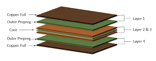
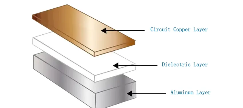
At high frequencies, transmission line theory governs medical PCB RF design, requiring 50-ohm impedance control to match transceiver outputs. Traces act as microstrips or striplines, where width, thickness, and substrate dielectric constant dictate characteristic impedance. Variations cause reflections, attenuating signals and increasing bit error rates. Multilayer stacks with dedicated RF layers isolate high-speed signals from digital noise.
Ground planes form the return path, minimizing inductance and shielding against crosstalk. Vias introduce discontinuities, so blind or buried types with back-drilling preserve integrity. Dielectric materials with low dissipation factor reduce insertion loss, critical for Bluetooth PCB design medical where range is limited. Engineers calculate stackups to maintain uniform fields, avoiding field fringing at edges.
Signal propagation follows Maxwell's equations, with wavelength shrinking to centimeters at 2.4 GHz, demanding sub-wavelength precision. Parasitics from components couple energy, necessitating pi-network matching for antennas. Thermal management prevents detuning, as dielectrics expand with heat.
Best Practices for Antenna Placement on Medical PCBs
Antenna placement on medical PCB begins with reserving edge or corner locations to maximize ground clearance and omnidirectional patterns. Keep-out zones, typically spanning the antenna length plus margins, must remain copper-free on all layers to prevent detuning. Positioning away from batteries or processors reduces loading from nearby dielectrics and noise sources. Simulations verify patterns, ensuring regulatory field strength limits.
For PCB trace antennas like inverted-F (IFA), bend traces smoothly to fit contours while preserving resonance. Feed and ground connections use short, wide paths for low loss. In Bluetooth PCB design medical, prioritize meander lines for compactness without sacrificing efficiency. Wi-Fi PCB design medical benefits from slot antennas in ground planes, leveraging chassis as radiator.
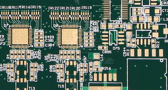
Partition the board into RF, analog, and digital zones, with stitching vias along boundaries. Guard traces shield sensitive paths, and decoupling capacitors stabilize supplies. Compliance with IPC-6018 for high-frequency boards ensures dimensional stability post-fabrication.
Ensuring Signal Integrity in Wireless Medical Devices
Signal integrity in wireless medical devices hinges on controlled impedance traces, verified through TDR measurements during prototyping. Minimize vias by routing on inner layers with plane references, and use mitered bends to reduce reflections. Differential pairs for balanced signals reject common-mode noise, ideal for Wi-Fi data lines.
Power integrity complements RF performance, with solid planes and ferrite beads filtering ripple. Decoupling networks near ICs supply transient currents, preventing ground bounce. EMI shielding via cans or pours contains emissions, aligning with medical EMC needs.
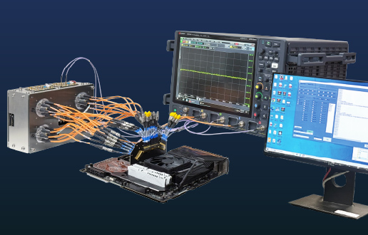
Crosstalk mitigation involves spacing rules: greater than 3 times trace width for parallel runs. Via fences along edges enhance isolation. Post-layout extraction models parasitics for final validation.
Challenges in High-Frequency Medical PCB Design and Practical Solutions
One challenge is form factor constraints, where small boards limit ground plane size, degrading antenna efficiency. Solutions include chip antennas with predefined keep-outs or flexible substrates for curved devices. Another issue is multilayer coupling, addressed by asymmetric stackups isolating RF layers.
Moisture absorption alters dielectrics, so bake-out and conformal coatings per IPC guidelines maintain consistency. Thermal vias under PAs dissipate heat without warping. For Bluetooth PCB design medical, adaptive power control algorithms compensate for detuning.
Wi-Fi PCB design medical faces higher harmonics, requiring low-pass filters and spread-spectrum modulation. Troubleshooting involves spectrum analysis to isolate spurs. Iterative DFMA reviews catch manufacturability issues early.
Conclusion
Designing medical PCBs for high-frequency wireless communication demands meticulous attention to RF principles, antenna placement, and signal integrity. Strategic practices like edge antenna positioning, impedance control, and partitioned layouts ensure reliable Bluetooth and Wi-Fi performance. Adhering to IPC Class 3 and IEC 60601 elevates designs to mission-critical standards. Engineers achieve this by simulating early, partitioning zones, and validating prototypes. These approaches not only optimize wireless medical devices but also future-proof against evolving protocols.
FAQs
Q1: What are the key considerations for medical PCB RF design at 2.4 GHz?
A1: Medical PCB RF design at 2.4 GHz prioritizes 50-ohm impedance traces, solid ground planes, and low-loss dielectrics to combat skin effect and dielectric losses. Antenna placement on medical PCB edges maximizes clearance, while via minimization preserves signal integrity. Compliance with IPC-6018 ensures high-frequency stability. Partitioning RF from digital sections reduces crosstalk for reliable operation.
Q2: How does antenna placement on medical PCB affect Bluetooth performance?
A2: Antenna placement on medical PCB significantly impacts Bluetooth range and efficiency by influencing ground coupling and radiation patterns. Corners or edges with copper-free keep-outs prevent detuning, ideal for Bluetooth PCB design medical. Simulations optimize feed points, ensuring low VSWR. Proximity to metal enclosures requires detuning adjustments for consistent packet delivery.
Q3: Why is signal integrity critical in Wi-Fi PCB design medical?
A3: Signal integrity in wireless medical devices prevents data corruption in Wi-Fi PCB design medical, where high data rates amplify reflections and jitter. Controlled impedance, mitered corners, and shielding maintain eye diagrams. Ground stitching isolates noise, supporting IEC 60601 EMC. Proper decoupling ensures clean power for transceivers.
Q4: What role do standards play in medical PCB RF design?
A4: Standards like IPC-6012 and IEC 60601 guide medical PCB RF design by specifying reliability, impedance tolerances, and safety. They mandate Class 3 quality for high-frequency boards, ensuring signal integrity in wireless medical devices. Consistent application minimizes field failures and eases certification.