 ALLPCB


Introduction
Printed circuit board finishes protect copper traces from oxidation and ensure reliable soldering during assembly. Among the common options, HASL and ENIG stand out for their widespread use in various projects. HASL PCB finish involves applying molten solder and leveling it with hot air, creating a thick, durable coating. ENIG PCB finish uses a nickel barrier topped with a thin gold layer through electroless plating. Choosing between ENIG vs HASL depends on your project's needs, such as soldering ease, cost, and environmental exposure. This PCB project guide compares these finishes to help electronic hobbyists make informed decisions.
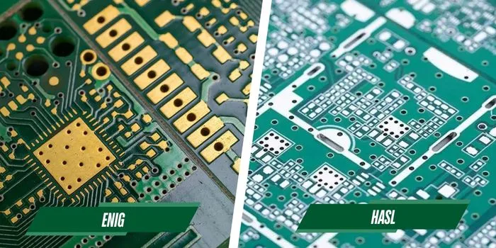
What Is HASL PCB Finish?
HASL, or Hot Air Solder Leveling, coats PCB pads with solder alloy, typically tin-lead or lead-free variants. The process dips the board in molten solder, then blasts it with hot air to remove excess, leaving a uniform layer. This results in a matte or shiny surface that matches common soldering materials. HASL excels in solderability because the finish is pure solder, making it ideal for hand soldering in hobby setups. It withstands multiple thermal cycles without significant degradation. However, the uneven thickness can pose challenges for fine-pitch components.
HASL remains popular due to its low cost and availability in most fabrication services. Hobbyists appreciate its forgiving nature during rework, as excess solder flows easily. The finish complies with IPC standards for solder joint reliability in through-hole assemblies. Shelf life extends up to two years under proper storage, though oxidation may occur over time. For prototypes, HASL provides a straightforward option without complex processing steps.
What Is ENIG PCB Finish?
ENIG, or Electroless Nickel Immersion Gold, deposits a nickel-phosphorus layer followed by a thin immersion gold cap. The electroless process requires no electricity, allowing uniform coverage on complex board geometries. Nickel acts as a diffusion barrier, while gold prevents oxidation and ensures excellent wettability. This finish suits surface-mount technology with tight tolerances, common in modern hobby projects. ENIG maintains flatness, avoiding issues like bridging in dense layouts.
The gold layer, typically 0.05 to 0.2 micrometers thick, offers superior corrosion resistance in humid environments. Black pad issues, where nickel corrodes under gold, have been mitigated in modern formulations per IPC-4552 specifications. ENIG boards exhibit a shelf life exceeding two years, making them reliable for inventory storage. Hobbyists value its lead-free compliance and compatibility with no-clean fluxes. Processing involves multiple chemical baths, increasing lead times compared to simpler finishes.
PCB Finish Comparison: ENIG vs HASL
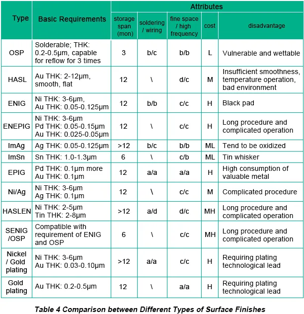
ENIG vs HASL reveals distinct trade-offs in performance characteristics. HASL provides thicker solder layers, around 5 to 25 micrometers, promoting strong mechanical bonds in through-hole joints. ENIG offers precise, thin coatings ideal for ball grid arrays and fine-pitch QFNs. Solderability remains high for both, but ENIG wets faster with lead-free solders due to gold's properties.
Cost favors HASL, which uses inexpensive materials and quick processing. ENIG demands pricier chemicals and baths, raising expenses by 20 to 50 percent for small runs. Shelf life tilts toward ENIG, resisting oxidation longer than HASL's solder surface. In thermal shock tests per IPC-6012, HASL handles higher temperatures, while ENIG excels in humidity.
- Thickness: HASL 5–25 μm (uneven); ENIG Ni 3–6 μm, Au 0.05–0.2 μm
- Solderability: HASL excellent for hand soldering; ENIG superior for SMT reflow
- Shelf Life: HASL 1–2 years; ENIG >2 years
- Cost: HASL low; ENIG higher
- Flatness: HASL moderate (peaks/valleys); ENIG excellent (planar)
- Best For: HASL prototypes and through-hole; ENIG fine-pitch and high-reliability
Environmental factors influence choice, with ENIG better for harsh conditions and HASL sufficient for benign hobby use.
Key Factors to Consider in Your PCB Project Guide
Electronic hobbyists must weigh assembly methods when selecting between ENIG vs HASL. Hand soldering favors HASL's abundant solder supply, reducing bridging risks during iron work. Reflow ovens pair well with ENIG's flat surface, ensuring consistent melting across pads. Component pitch matters, as HASL's topography challenges pitches below 0.5 mm.
Budget constraints often steer hobby projects to HASL for quick prototypes. Volume production may justify ENIG's premium for yield improvements. Compliance with RoHS pushes toward lead-free HASL or ENIG equally. Test your design's exposure, using HASL for indoor gadgets and ENIG for outdoor sensors.
Storage and rework play roles too. ENIG's longevity suits infrequent builds, while HASL allows easy desoldering. Consult fabrication quotes early to balance specs. Following J-STD-001 guidelines ensures joints meet reliability thresholds regardless of finish.
Best Practices for HASL and ENIG in Hobby Projects
Store unfinished boards in nitrogen-purged bags to maximize shelf life for either finish. Preheat HASL boards gently before soldering to avoid thermal shock. Use flux compatible with ENIG to prevent nickel dissolution. Inspect HASL for solder beads post-fabrication, removing them with a hot air station.
For ENIG, avoid excessive immersion time in fluxes per IPC-4552 to preserve gold integrity. Test solder joints with continuity checks and visual exams. Hybrid approaches, like HASL on through-holes and ENIG on SMT pads, work for mixed assemblies but increase complexity. Document your finish choice based on project trials for future reference.
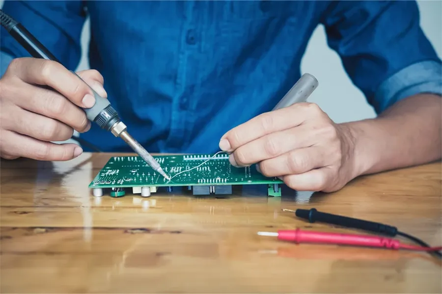
Troubleshoot common issues systematically. HASL bridging resolves with wick and flux, while ENIG non-wetting signals contamination, cleaned via ultrasonic baths. Simulate reflow profiles matching your oven capabilities. These steps align with factory-driven insights for hobby success.
Conclusion
ENIG vs HASL boils down to project specifics like pitch, budget, and assembly style. HASL PCB finish delivers cost-effective reliability for hand-soldered prototypes, thriving in forgiving hobby workflows. ENIG PCB finish shines in precision SMT with extended durability. This PCB finish comparison equips you to select wisely, enhancing project outcomes. Experiment with small runs to validate choices, ensuring robust electronics builds.
FAQs
Q1: What is the main difference in ENIG vs HASL for hobby projects?
A1: ENIG provides a thin, flat nickel-gold layer for fine-pitch surface-mount components, offering better shelf life and corrosion resistance. HASL applies a thicker solder coat leveled by hot air, suiting hand soldering and through-hole designs with lower costs. Choose ENIG for reflow-heavy builds and HASL for quick prototypes. Both ensure good solderability when stored properly.
Q2: Is HASL PCB finish suitable for lead-free soldering?
A2: Yes, lead-free HASL uses tin-silver-copper alloys compatible with modern solders. It maintains wettability similar to traditional versions, though higher reflow temperatures require adjusted profiles. Hobbyists find it reliable for prototypes, matching ENIG in joint strength per soldering standards. Avoid mixing alloys to prevent brittle intermetallics.
Q3: When should electronic hobbyists pick ENIG PCB finish?
A3: Opt for ENIG in projects with tight pad spacing under 0.5 mm or humid environments needing long shelf life. Its planar surface prevents bridging in dense SMT layouts. Higher cost pays off for reusable designs or high-reliability gadgets. HASL suffices for coarser pitches and budget constraints.
Q4: How does PCB finish comparison affect rework in projects?
A4: HASL eases rework due to its solder-rich surface, allowing easy addition or removal with basic tools. ENIG requires careful flux use to avoid damaging the thin gold, but supports clean desoldering. Both allow multiple cycles if following thermal guidelines. Test small areas first for best results.





