Introduction
Metal Core Printed Circuit Boards (MCPCBs) are increasingly vital in radio frequency (RF) applications due to their superior thermal management and structural stability. As RF systems push into higher frequencies for telecommunications, aerospace, and automotive radar, the demand for reliable high frequency PCB materials grows. However, integrating MCPCBs into RF designs presents unique challenges such as maintaining signal integrity RF PCB, achieving precise impedance matching MCPCB, and reducing losses RF PCB. This article explores the intricacies of RF MCPCB design, delving into the technical hurdles engineers face and offering practical solutions to optimize performance. Written for electrical engineers, this content aims to provide actionable insights into material selection, layout strategies, and best practices for high frequency applications.
What Are Metal Core PCBs and Why Do They Matter in RF Applications
Metal Core PCBs are specialized circuit boards with a metal base layer, typically aluminum or copper, which enhances thermal dissipation. In RF applications, where high power and high frequency signals generate significant heat, MCPCBs offer a robust solution to prevent thermal degradation of components. Their ability to manage heat effectively is crucial for maintaining signal integrity RF PCB, especially in systems operating above 1 GHz, such as 5G infrastructure or satellite communications. Beyond thermal benefits, the metal core provides mechanical strength, reducing the risk of board warping under stress. For engineers working on RF MCPCB design, understanding the interplay between thermal performance and electrical characteristics is essential to ensure reliable operation in demanding environments.
Technical Challenges in RF MCPCB Design
Material Selection for High Frequency Performance
Selecting appropriate high frequency PCB materials for MCPCBs is a primary challenge. Standard dielectric materials often exhibit high dielectric losses at RF frequencies, impacting signal quality. The dielectric constant and loss tangent of the material must be carefully evaluated to minimize signal attenuation. Additionally, the thermal conductivity of the metal core must align with the dielectric layer to avoid uneven heat distribution, which can alter electrical properties and affect impedance matching MCPCB. Engineers must balance these factors to ensure compatibility with RF signal requirements while maintaining thermal efficiency.
(Insert image: "High Frequency PCB Material Layers" · ALT: "Cross section of MCPCB showing metal core and dielectric layers")
Signal Integrity Issues in RF Environments
Maintaining signal integrity RF PCB is a critical concern in high frequency designs. RF signals are prone to interference, crosstalk, and reflections due to the short wavelengths involved. In MCPCBs, the proximity of the metal core can introduce parasitic capacitance, distorting signal paths. Furthermore, variations in the dielectric thickness or material properties can lead to inconsistent signal propagation, causing phase shifts or amplitude loss. These issues become more pronounced as frequencies increase, making precise control over board layout and material uniformity essential for RF MCPCB design.
Impedance Matching Complexities
Achieving impedance matching MCPCB in RF applications is complicated by the unique structure of metal core boards. The metal base can influence the characteristic impedance of transmission lines, requiring careful trace width and spacing calculations. Mismatches in impedance lead to signal reflections, reducing power transfer efficiency and degrading performance. Additionally, the transition between different layers or components on the PCB can introduce discontinuities, further complicating impedance control. Engineers must address these factors to ensure seamless signal transmission across the board.
Thermal and Electrical Loss Management
Reducing losses RF PCB is a significant challenge when using MCPCBs in high frequency systems. Dielectric losses, conductor losses, and radiation losses all contribute to signal degradation. The metal core, while excellent for heat dissipation, can exacerbate conductor losses if not properly isolated from signal traces. Thermal expansion differences between the metal core and dielectric layers may also induce stress, potentially causing micro cracks or delamination over time. Managing these losses requires a combination of material optimization and strategic design techniques.
(Insert image: "Thermal Distribution on MCPCB" · ALT: "Heat map showing thermal dissipation on a metal core PCB")
Practical Solutions for RF MCPCB Design
Optimizing Material Choices
To address material challenges, engineers should prioritize low loss dielectric materials with stable dielectric constants across the target frequency range. Materials with low dissipation factors are ideal for reducing losses RF PCB. Additionally, selecting a metal core with high thermal conductivity, such as aluminum, can enhance heat dissipation without significantly impacting electrical performance. It is also important to ensure compatibility between the dielectric and metal layers to prevent thermal mismatch during operation. Consulting industry standards like IPC-6012E for material performance specifications can guide the selection process.
Enhancing Signal Integrity
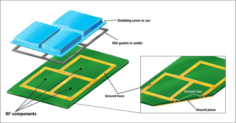
To maintain signal integrity RF PCB, designers should implement controlled impedance traces and minimize the use of vias, which can act as points of signal reflection. Ground planes should be strategically placed to shield RF signals from interference caused by the metal core. Using simulation tools to model signal behavior before fabrication can help identify potential issues in the layout. Additionally, maintaining uniform dielectric thickness across the board prevents variations in signal propagation, ensuring consistent performance in high frequency environments.
(Insert image: "RF Signal Trace Layout" · ALT: "PCB layout showing controlled impedance traces for RF signals")
Achieving Effective Impedance Matching
For impedance matching MCPCB, precise calculation of trace dimensions based on the dielectric properties and metal core influence is necessary. Designers can use microstrip or stripline configurations to control characteristic impedance. Incorporating matching networks, such as stub filters or lumped elements, can further fine tune impedance at critical points. Adhering to guidelines from standards like IPC-A-600K for trace geometry and tolerances ensures manufacturing consistency, reducing the risk of mismatches during production.
Strategies for Reducing Losses
Reducing losses RF PCB involves multiple approaches. Using high conductivity materials for traces minimizes conductor losses, while selecting low loss dielectrics addresses dielectric losses. To mitigate radiation losses, engineers should avoid sharp bends in traces and maintain proper spacing between signal lines to prevent crosstalk. Thermal management can be improved by optimizing the metal core thickness and ensuring adequate heat sinking. Regular testing during the design phase, aligned with standards like IPC-6012E, helps identify and address loss contributors early.
(Insert image: "RF PCB Loss Testing Setup" · ALT: "Equipment setup for measuring signal loss on RF PCB")
Troubleshooting Common Issues in RF MCPCB Applications
In practical scenarios, engineers often encounter unexpected signal degradation or thermal hotspots during RF MCPCB testing. A systematic approach to troubleshooting can resolve these issues efficiently. Start by verifying material properties against design specifications, as deviations in dielectric constant or loss tangent can impact performance. Use network analyzers to measure impedance mismatches and adjust trace layouts accordingly. If thermal issues arise, inspect the bonding between the metal core and dielectric layer for defects, as poor adhesion can hinder heat transfer. Documenting test results and comparing them against benchmarks from standards like IPC-A-600K ensures consistent quality control.
(Insert image: "Network Analyzer Testing RF PCB" · ALT: "Using a network analyzer to test signal integrity on RF PCB")
Conclusion
Metal Core PCBs offer significant advantages for RF applications through effective thermal management and structural durability. However, challenges in RF MCPCB design, including material selection, signal integrity RF PCB, impedance matching MCPCB, and reducing losses RF PCB, require careful consideration. By leveraging high frequency PCB materials with low loss characteristics, optimizing trace layouts, and adhering to industry standards, engineers can overcome these hurdles. The solutions outlined in this article provide a roadmap for designing robust MCPCBs tailored to high frequency systems, ensuring reliable performance in demanding applications.
FAQs
Q1: What are the key considerations for selecting high frequency PCB materials in RF MCPCB design?
A1: Selecting high frequency PCB materials for RF MCPCB design involves evaluating dielectric constant, loss tangent, and thermal conductivity. Materials with low dissipation factors minimize signal loss, while compatibility with the metal core prevents thermal mismatch. Stability across frequency ranges is crucial for consistent performance. Consulting industry standards ensures materials meet the necessary electrical and thermal requirements for RF applications.
Q2: How can signal integrity RF PCB be maintained in metal core boards?
A2: Maintaining signal integrity RF PCB in metal core boards requires controlled impedance traces, minimal vias, and strategic ground plane placement. Shielding signals from the metal core reduces interference, while uniform dielectric thickness prevents propagation issues. Simulation tools help predict signal behavior, allowing adjustments before fabrication. Regular testing during design validates performance and identifies potential disruptions early.
Q3: What techniques improve impedance matching MCPCB in high frequency applications?
A3: Improving impedance matching MCPCB involves calculating trace dimensions based on dielectric properties and metal core effects. Microstrip or stripline configurations help control impedance, while matching networks fine tune critical points. Adhering to manufacturing tolerances from recognized standards ensures consistency. Testing with network analyzers during prototyping can detect and correct mismatches for optimal signal transfer.
Q4: How can engineers focus on reducing losses RF PCB in metal core designs?
A4: Reducing losses RF PCB in metal core designs requires using high conductivity trace materials and low loss dielectrics. Avoiding sharp trace bends and maintaining proper spacing minimizes radiation and crosstalk losses. Optimizing metal core thickness enhances thermal management. Routine testing aligned with industry guidelines helps identify loss sources, enabling targeted improvements during the design process.
References
IPC-6012E — Qualification and Performance Specification for Rigid Printed Boards. IPC, 2020.
IPC-A-600K — Acceptability of Printed Boards. IPC, 2020.
 ALLPCB


