Introduction
Flexible printed circuit boards, often termed flex PCBs, are transforming the telecommunications industry with their unique ability to bend and adapt to compact designs. As devices become smaller and more complex, the demand for bendable PCB solutions grows, especially in applications requiring high-density flex PCB layouts. This article explores the critical role of flexible PCB design in telecommunications, delving into technical principles, practical applications, and adherence to industry standards. Aimed at electrical engineers, this piece offers structured insights into how telecommunications flex PCB solutions address modern connectivity challenges. From wearable devices to advanced networking equipment, understanding flex PCB applications is essential for engineers seeking innovative and reliable designs in a rapidly evolving field.
What Are Flexible PCBs and Why Do They Matter in Telecommunications?
Flexible PCBs are circuit boards made from pliable materials like polyimide, allowing them to bend, fold, or twist without damaging the conductive traces. Unlike rigid boards, they offer significant advantages in space constrained environments, a common requirement in telecommunications equipment. Their lightweight nature and adaptability make them ideal for applications where traditional boards fail to fit or perform. In telecommunications, the relevance of flex PCB applications lies in enabling compact designs for devices such as smartphones, antennas, and base station components.
The ability to integrate high-density flex PCB layouts into tight spaces ensures that modern devices maintain performance while shrinking in size. This technology supports the industry's push toward faster data transmission and miniaturization, aligning with the needs of 5G networks and IoT ecosystems. For engineers, recognizing the potential of bendable PCB solutions means unlocking new possibilities in product design and system efficiency.
Technical Principles of Flexible PCB Design
Flexible PCB design hinges on material selection, layer stack up, and mechanical properties. The base substrate, often polyimide, provides durability under repeated bending. Conductive traces, typically copper, must be thin yet robust to prevent cracking during flexing. Standards such as IPC-2223E, which governs sectional design for flexible and rigid flex boards, outline critical parameters like bend radius and trace width to ensure reliability.
Bend radius is a key factor, defined as the minimum radius a flex PCB can withstand without stress. IPC-2223E recommends a ratio of at least 10:1 for dynamic flexing to avoid fatigue. Static applications may tolerate tighter bends, but engineers must balance this with material limits. Adhesives and coverlays also play a role, protecting traces while maintaining flexibility. For telecommunications flex PCB designs, high frequency signal integrity is vital. Materials with low dielectric constants are often chosen to minimize signal loss, especially in 5G applications.
Thermal management poses another challenge. Flex PCBs in telecommunications often operate in confined spaces with limited airflow. Engineers must consider heat dissipation paths to prevent performance degradation. Compliance with standards like IPC-6013D, which specifies performance for flexible printed boards, ensures designs meet industry expectations for durability and electrical performance.
Applications of Flex PCBs in Telecommunications
Flex PCB applications in telecommunications span a wide range of devices and systems. In mobile devices, bendable PCB technology allows for intricate folding within tight enclosures, supporting features like foldable screens and compact camera modules. Antennas, often integrated into flex PCBs, benefit from the ability to conform to irregular shapes, optimizing signal reception in confined spaces.
Base stations and networking equipment utilize high-density flex PCB designs to manage complex interconnections. These boards reduce cable clutter, improving reliability and easing maintenance. Wearable communication devices, such as smartwatches, rely on flex PCBs to fit ergonomic designs while maintaining connectivity. The push for IoT integration further drives demand, as sensors and communication modules require lightweight, adaptable circuitry.
In 5G infrastructure, telecommunications flex PCB solutions are critical for high frequency signal routing. Their ability to handle dense layouts supports the miniaturization of components without sacrificing performance. Engineers must ensure these designs comply with standards like IPC-A-600K for acceptability of printed boards, guaranteeing quality in high stakes applications.
Best Practices for Designing Flexible PCBs in Telecommunications
Designing flexible PCBs for telecommunications requires a systematic approach to balance functionality and durability. First, define the application type, whether static or dynamic flexing, as this impacts material choice and bend radius. Refer to IPC-2223E for guidelines on minimum bend ratios and layer configurations to prevent mechanical failure.
Material selection is crucial. Polyimide substrates are standard for their thermal stability and flexibility, but engineers must specify thickness based on bending needs. Copper weight should be minimal for flexibility, yet sufficient for current carrying capacity. High-density flex PCB designs often require microvias and fine traces, so precision in layout is essential to avoid signal interference, especially in 5G contexts.
Signal integrity demands attention to impedance control. Matching trace geometry with dielectric properties minimizes losses, a concern in telecommunications flex PCB projects. Thermal vias or heat spreading layers can address heat buildup in confined designs. Always validate designs against standards like IPC-6013D to ensure performance under operational stress.
Prototyping and testing are non negotiable. Simulate bending cycles to identify weak points, aligning with IPC-6013D test methods. Iterative design adjustments based on test outcomes enhance reliability. Collaboration between design and manufacturing teams ensures that telecommunications flex PCB solutions transition smoothly from concept to production.
Challenges and Solutions in Telecommunications Flex PCB Implementation
Telecommunications flex PCB projects face unique challenges, including mechanical stress, signal degradation, and manufacturing precision. Repeated bending can lead to trace fatigue, especially in dynamic applications like foldable devices. Adhering to IPC-2223E guidelines for bend radius and material selection mitigates this risk. Reinforcing critical areas with stiffeners adds durability without compromising flexibility.
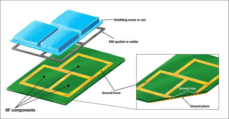
Signal degradation is a concern in high frequency telecommunications applications. Engineers must prioritize low loss materials and precise impedance matching to maintain data rates. Standards like IPC-A-600K provide criteria for trace quality, ensuring consistent electrical performance. Shielding layers can also reduce electromagnetic interference in dense layouts.
Manufacturing high-density flex PCB designs demands tight tolerances. Misalignment or material defects can lead to failures. Compliance with IPC-6013D ensures process control during fabrication, from lamination to etching. Partnering with fabrication teams early in the design phase helps address potential issues, streamlining production of bendable PCB solutions for telecommunications.
Conclusion
Flexible PCBs are a cornerstone of innovation in telecommunications, enabling compact, reliable designs for modern connectivity needs. From smartphones to 5G infrastructure, flex PCB applications address the industry's demand for miniaturization and performance. By understanding flexible PCB design principles and adhering to standards like IPC-2223E and IPC-6013D, engineers can create robust solutions for complex challenges. As telecommunications evolves, high-density flex PCB technology will remain pivotal, driving advancements in speed, efficiency, and device integration. This knowledge equips professionals to navigate the intricacies of bendable PCB implementation with confidence.
FAQs
Q1: How does flexible PCB design impact signal integrity in telecommunications?
A1: Flexible PCB design must prioritize impedance control and low loss materials to maintain signal integrity, especially for high frequency telecommunications applications. Standards like IPC-A-600K guide trace quality to minimize degradation. Proper layout and shielding reduce interference, ensuring reliable data transmission in compact devices.
Q2: What are the key considerations for bendable PCB use in 5G infrastructure?
A2: Bendable PCB solutions for 5G infrastructure require materials with low dielectric constants to handle high frequencies. Bend radius, as per IPC-2223E, must support dynamic flexing in tight spaces. High-density layouts are essential for compact designs, demanding precision to avoid signal loss or mechanical failure.
Q3: Why are high-density flex PCB layouts critical for modern telecommunications devices?
A3: High-density flex PCB layouts enable miniaturization in telecommunications devices by packing more components into limited spaces. They support complex interconnections in smartphones and base stations, maintaining performance. Adherence to standards like IPC-6013D ensures reliability under operational stress in dense configurations.
Q4: What standards govern flex PCB applications in telecommunications equipment?
A4: Flex PCB applications in telecommunications are governed by standards like IPC-2223E for design, IPC-6013D for performance, and IPC-A-600K for acceptability. These ensure mechanical durability, signal quality, and manufacturing precision, providing a framework for engineers to develop robust and efficient designs.
References
IPC-2223E — Sectional Design Standard for Flexible and Rigid-Flex Printed Boards. IPC, 2021.
IPC-6013D — Qualification and Performance Specification for Flexible and Rigid-Flex Printed Boards. IPC, 2017.
IPC-A-600K — Acceptability of Printed Boards. IPC, 2020.
 ALLPCB


