ALLPCB


Introduction
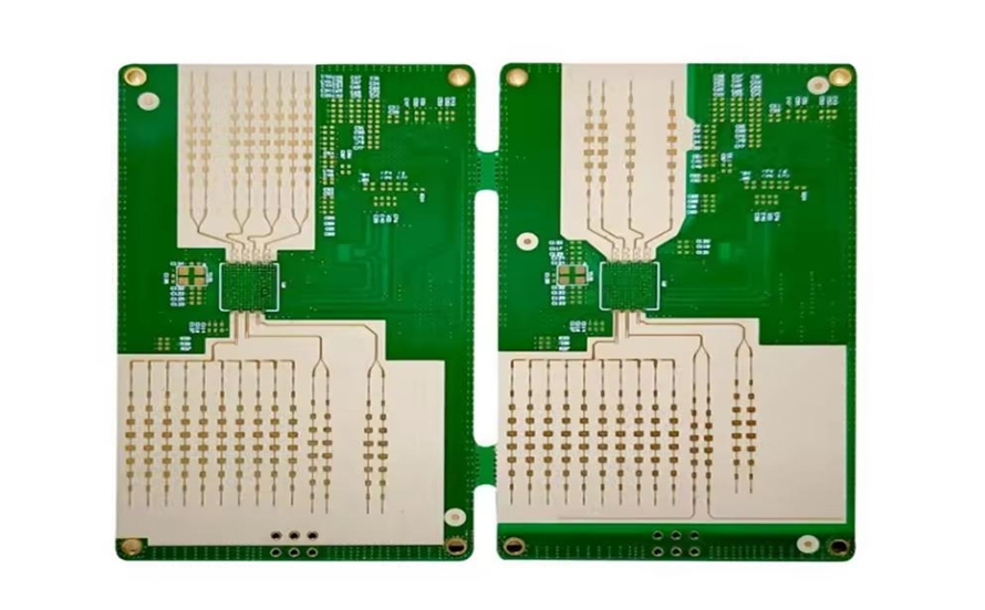
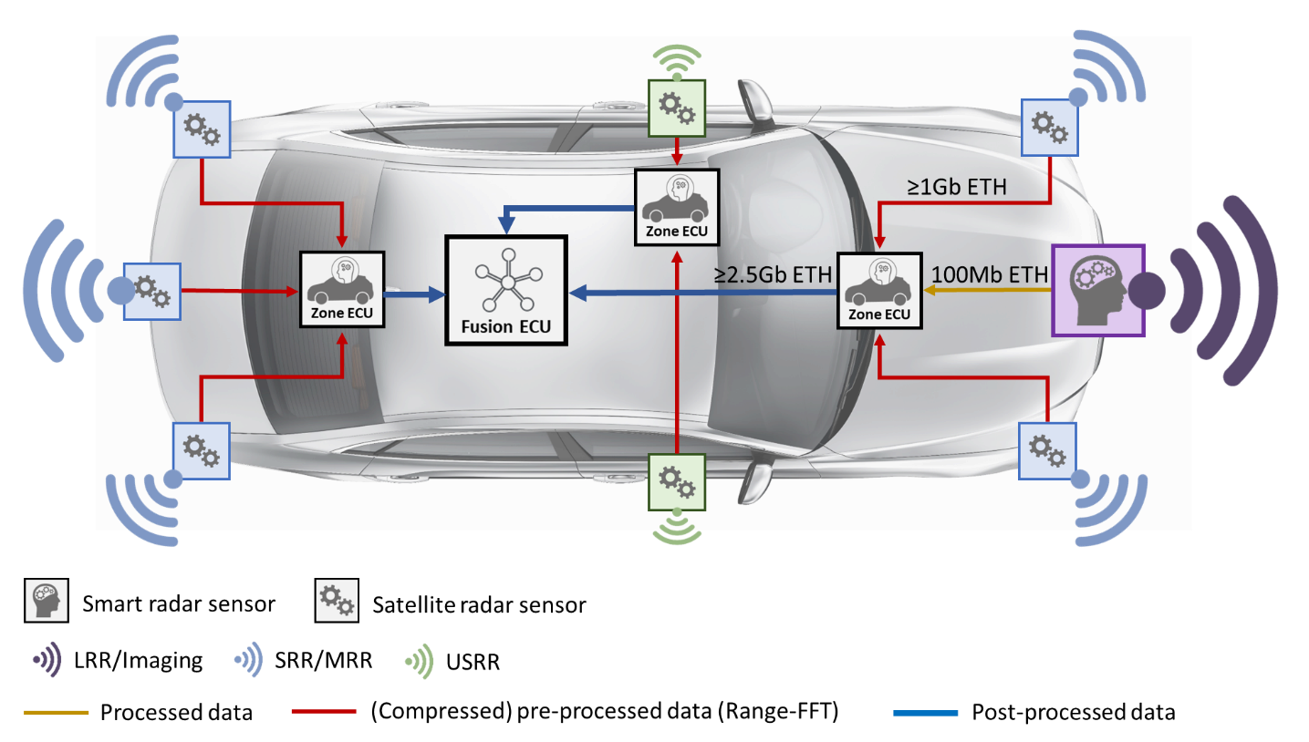
High-frequency automotive PCBs play a critical role in modern vehicles equipped with advanced driver-assistance systems (ADAS) and vehicle-to-everything (V2X) communication. These boards support radar sensors operating in millimeter-wave bands and communication modules handling high-data-rate signals. As automotive systems push toward higher frequencies to enable precise object detection and real-time data exchange, PCB designers face unique challenges in maintaining signal integrity amid harsh environmental conditions. Automotive radar PCBs must deliver low-latency performance for collision avoidance, while automotive communication PCBs ensure reliable connectivity in dynamic scenarios. Effective high-frequency material selection becomes essential to minimize losses and control impedance. This article explores the design and material hurdles in automotive PCB high-frequency design, offering structured insights for engineers tackling these demands.
Why High-Frequency Automotive PCBs Matter
Automotive radar PCBs operate at frequencies where traditional materials falter, demanding specialized substrates to preserve signal strength over short distances. These boards enable 360-degree sensing for autonomous driving, where even minor signal degradation can compromise safety. Similarly, automotive communication PCBs support protocols requiring gigabit speeds, integrating antennas directly onto the board for compact designs. The shift to software-defined vehicles amplifies the need for robust high-frequency performance, as PCBs bridge RF front-ends with digital processing units. Engineers must prioritize signal loss reduction and precise impedance matching to meet system-level requirements. Failure to address these aspects results in increased bit error rates or reduced detection ranges, underscoring the relevance of optimized automotive PCB high-frequency design.
In production environments, these PCBs undergo stringent reliability testing to withstand vibration, thermal cycling, and humidity typical of automotive use. High-frequency signals exacerbate issues like crosstalk and reflections, making material choices pivotal from the outset. As vehicle electrification accelerates, integrating power and high-speed signals on the same board adds complexity. Designers benefit from understanding how dielectric properties influence propagation delay and attenuation. This foundation ensures compliance with performance benchmarks while supporting scalable manufacturing.
Key Technical Principles in High-Frequency Design
At high frequencies, electromagnetic waves interact strongly with PCB materials and geometries, leading to phenomena like skin effect and dielectric polarization losses. Conductor losses dominate due to current confinement to trace surfaces, while dielectric losses arise from energy dissipation in the substrate. Automotive radar PCBs, handling millimeter-wave signals, require traces with controlled widths to mitigate these effects. Automotive communication PCBs face similar issues but often at slightly lower bands, where multi-layer stackups introduce additional coupling risks. Engineers model these using field solvers to predict field distributions accurately. Proper grounding planes shield sensitive traces, reducing radiation losses.
Impedance matching forms the cornerstone of automotive PCB high-frequency design, as mismatches cause standing waves that degrade return loss. Characteristic impedance depends on trace width, thickness, dielectric height, and material constants. Variations in manufacturing tolerances can shift impedance by several ohms, necessitating tight process controls. Signal loss reduction involves selecting substrates with stable dielectric constants across frequencies and temperatures. Low dissipation factors prevent phase distortion, crucial for phase-array radars. Thermal expansion mismatches between layers can warp boards, altering dimensions post-fabrication.
IPC-6012 provides qualification criteria for rigid printed boards, including those for high-reliability automotive applications, emphasizing electrical performance under stress.
High-Frequency Material Selection Challenges
High-frequency material selection prioritizes substrates with low dielectric constant (Dk) for faster signal speeds and low dissipation factor (Df) to curb attenuation. Automotive environments demand materials stable from minus forty degrees Celsius to over one hundred twenty-five degrees Celsius, resisting moisture absorption that swells dielectrics. Reinforced composites offer mechanical robustness, balancing RF performance with drillability for vias. Hybrid stackups combine low-loss cores with standard prepregs for cost efficiency, though interfaces pose adhesion risks. Engineers evaluate tan delta curves versus frequency to predict losses accurately. Coefficient of thermal expansion matching prevents delamination in power-dense designs.
Ceramic-filled polymers provide moderate Dk stability, suitable for automotive radar PCBs where antenna integration requires precise patterning. For automotive communication PCBs, materials with filled epoxy offer higher Tg for reflow compatibility. Fabrication challenges include laser drilling for blind vias, as high-frequency signals demand via stubs minimization. Plating uniformity affects surface roughness, impacting conductor losses via skin depth reduction. Prepreg flow control ensures uniform resin distribution in multi-layer presses. Material datasheets guide selection, but empirical testing validates performance in assemblies.
IPC-4103 specifies requirements for high-frequency laminates, covering specification sheets for RF-optimized base materials.
Signal Loss Reduction and Impedance Matching Strategies
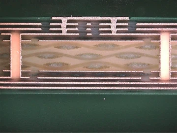
Signal loss reduction in automotive PCB high-frequency design hinges on smoothing conductor surfaces and optimizing dielectric interfaces. Increasing trace thickness counters skin effect but raises impedance, requiring width adjustments. Embedded ground planes beneath signal layers absorb evanescent fields, cutting radiation. For automotive radar PCBs, microstrip or stripline configurations isolate signals effectively. Automotive communication PCBs benefit from differential pairs with symmetric routing to reject common-mode noise. Vias introduce discontinuities; back-drilling or filled vias mitigate stubs.
Impedance matching employs controlled depth routing and soft-gold finishes for low insertion loss connectors. Stackup symmetry aids symmetry in field patterns, stabilizing Z0. Simulations iterate geometries before layout commitment. Tolerance stacking in fabrication demands statistical process control for plus or minus ten percent impedance holds. Environmental aging shifts Dk, so accelerated life tests predict long-term drift. Pairing with via fences suppresses slotline modes in transitions.
Practical Best Practices for Design and Fabrication
Start with stackup planning, allocating low-loss layers to critical signals while using cost-effective cores for power. Route high-speed traces on inner layers with ground references, adhering to length-matching for clocks. Minimize vias through direct chip attach where feasible, reducing inductance. Automotive PCB high-frequency design thrives on design rule checks for bend radii exceeding three times line width. Fabricators apply plasma cleaning for residue-free surfaces, enhancing adhesion.
Qualification per IPC-A-600 ensures visual and dimensional acceptability, catching defects early. Thermal vias under RFICs dissipate heat, preventing hot spots that degrade Df. Controlled impedance test coupons on panels verify production capability. For signal loss reduction, wider traces on outer layers leverage air dielectrics. Iterative prototyping refines models against measurements. Collaboration between design and fab teams aligns expectations on tolerances.
Conclusion
High-frequency automotive PCBs demand meticulous attention to material properties, geometry control, and process discipline to excel in radar and communication roles. Key challenges like signal loss and impedance mismatches yield to low-Df substrates, precise stackups, and verification protocols. Automotive radar PCBs and automotive communication PCBs benefit from these strategies, ensuring reliability in demanding applications. Engineers adopting structured approaches achieve superior performance without excessive cost. Future designs will leverage evolving materials for even higher bands, solidifying PCB's role in connected vehicles.
FAQs
Q1: What factors drive high-frequency material selection for automotive radar PCBs?
A1: High-frequency material selection focuses on low dielectric constant and dissipation factor to minimize propagation delay and attenuation. Automotive radar PCBs require thermal stability and low moisture uptake for reliable mmWave performance. Mechanical strength supports vibration resistance, while processability aids fabrication. Engineers balance RF metrics with cost through hybrid constructions. This ensures signal integrity across operating temperatures.
Q2: How does impedance matching impact automotive PCB high-frequency design?
A2: Impedance matching prevents reflections that distort signals in automotive PCB high-frequency design. Consistent characteristic impedance relies on precise trace dimensions and dielectric heights. Tolerances below ten percent demand controlled fab processes. Simulations guide layouts, with coupons confirming production Z0. Mismatches amplify losses, critical for radar and communication systems.
Q3: What techniques reduce signal loss in automotive communication PCBs?
A3: Signal loss reduction in automotive communication PCBs involves low-roughness conductors and low-Df dielectrics. Ground planes shield traces, while symmetric routing cuts crosstalk. Via optimization eliminates stubs contributing to attenuation. Surface finishes minimize skin effect impacts. These practices maintain data rates in high-speed links.
Q4: Why follow IPC standards in high-frequency automotive PCB fabrication?
A4: IPC standards like IPC-6012 ensure qualification for electrical and mechanical performance in harsh automotive conditions. They define acceptance criteria, aiding consistency across suppliers. High-frequency designs benefit from material specs in IPC-4103. Compliance reduces field failures, supporting long-term reliability.