ALLPCB


In the fast-paced world of electronics, designing compact and efficient devices is more important than ever. If you're looking to master PCB stackup design for high density, ensure impedance control in multi-layer boards, maintain signal integrity in dense PCBs, or achieve a cost-effective multi-layer stackup, you're in the right place. This guide will walk you through the essentials of multi-layer PCB stackup design, offering practical tips and detailed insights to help you create high-performing circuit boards.
At its core, a multi-layer PCB stackup is the arrangement of conductive and insulating layers in a printed circuit board. A well-designed stackup can significantly improve performance, reduce noise, and save costs, especially in dense, high-speed applications. In this deep dive, we'll explore the fundamentals, design considerations, and best practices to unlock the full potential of your PCB designs.
What Is Multi-Layer PCB Stackup Design?
A multi-layer PCB consists of multiple layers of conductive material (usually copper) separated by insulating layers (dielectrics). The "stackup" refers to how these layers are arranged. For high-density designs, a proper stackup is critical to fit more components into a smaller space while maintaining functionality. It also plays a huge role in controlling impedance, ensuring signal integrity, and managing electromagnetic interference (EMI).
Think of the stackup as the foundation of your PCB. A poorly planned stackup can lead to signal delays, crosstalk, or even complete failure of the board. On the other hand, a carefully designed stackup can optimize performance and reduce manufacturing costs. Whether you're working on a 4-layer board for a simple consumer device or a 12-layer board for a high-speed server, understanding stackup design is key.
Why Multi-Layer PCB Stackup Matters for High-Density Designs
In high-density PCB designs, space is at a premium. Engineers often need to pack more components and traces into smaller areas, which increases the risk of interference and signal loss. A well-thought-out stackup addresses these challenges by:
- Providing dedicated layers for power and ground to reduce noise.
- Allowing tighter routing of signal traces for compact designs.
- Ensuring consistent impedance for high-speed signals.
- Minimizing crosstalk between adjacent traces and layers.
For instance, in a typical 6-layer PCB for a high-density application, you might dedicate the top and bottom layers to signals, the inner layers to power and ground planes, and additional layers for critical high-speed signals. This arrangement helps isolate sensitive signals and maintain a clean power supply.
Key Considerations for PCB Stackup Design in High-Density Applications
Designing a stackup for a high-density PCB requires balancing several factors. Let's break down the most important considerations to ensure your design performs well.
1. Layer Count and Arrangement
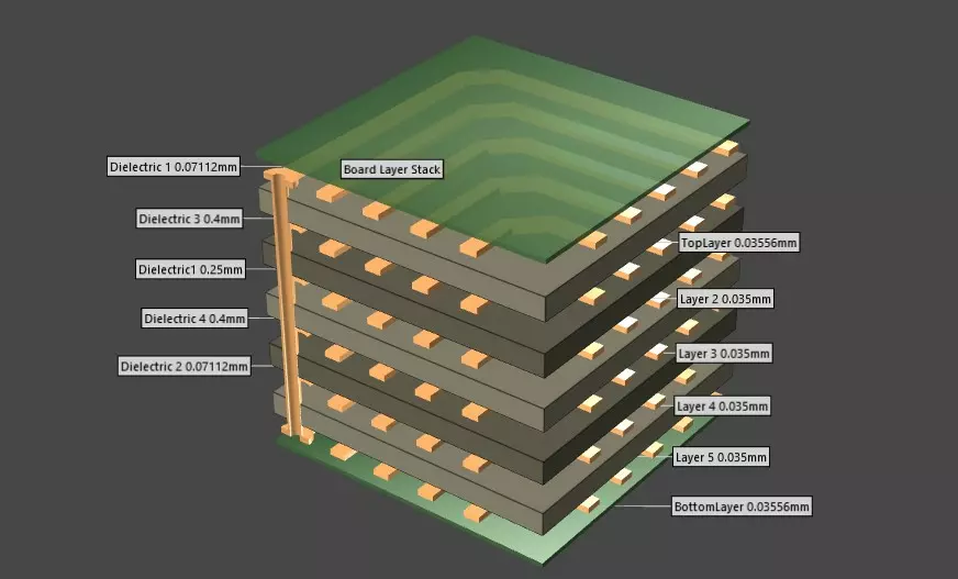
The number of layers in your PCB depends on the complexity and density of your design. A 4-layer board might suffice for simpler projects, while high-density or high-speed designs often require 8, 10, or even more layers. The arrangement of these layers is just as important. A common practice is to place power and ground planes adjacent to signal layers to provide a stable reference and reduce EMI.
For example, in an 8-layer board, a typical stackup might look like this:
- Layer 1: Top Signal
- Layer 2: Ground Plane
- Layer 3: Signal
- Layer 4: Power Plane
- Layer 5: Power Plane
- Layer 6: Signal
- Layer 7: Ground Plane
- Layer 8: Bottom Signal
This setup ensures that every signal layer has a nearby reference plane, which is crucial for maintaining signal integrity in dense PCBs.
2. Impedance Control in Multi-Layer Boards
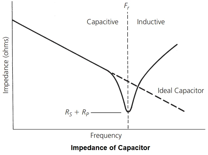
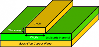
Impedance control is a critical factor in high-speed designs. It ensures that signals travel along traces without significant reflections or losses. To achieve proper impedance control in multi-layer boards, you need to carefully select the dielectric material, control the trace width and spacing, and maintain consistent layer thickness.
For instance, a common target impedance for high-speed signals like USB or HDMI is 50 ohms for single-ended traces or 100 ohms for differential pairs. Achieving this requires precise calculations based on the dielectric constant (Dk) of the material, typically around 4.2 for standard FR-4, and the geometry of the traces. Software tools can help simulate and verify impedance values during the design phase.
3. Signal Integrity in Dense PCBs
Signal integrity refers to the quality of an electrical signal as it travels through the PCB. In dense designs, maintaining signal integrity in dense PCBs is challenging due to the close proximity of traces, which can lead to crosstalk and interference. A good stackup minimizes these issues by:
- Keeping high-speed signal layers close to ground planes to reduce loop inductance.
- Separating sensitive analog signals from noisy digital signals on different layers.
- Using continuous ground planes to provide a low-impedance return path.
For example, in high-speed applications, a signal traveling at 5 GHz can experience significant loss if the return path is interrupted by vias or splits in the ground plane. A solid ground plane directly beneath the signal layer can reduce this risk and keep the signal clean.
4. Thermal Management
High-density designs often generate more heat due to the concentration of components. A good stackup can help dissipate heat by incorporating thermal vias and placing power planes strategically to spread heat evenly. Using materials with higher thermal conductivity can also improve performance in heat-sensitive applications.
Cost-Effective Multi-Layer Stackup Techniques
While performance is critical, cost is always a concern in PCB design. Achieving a cost-effective multi-layer stackup doesn't mean cutting corners—it means making smart choices that balance performance and budget. Here are some techniques to keep costs down without sacrificing quality:
1. Optimize Layer Count
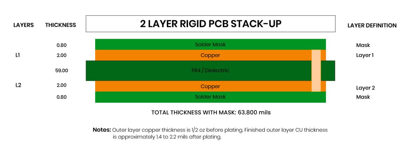
Every additional layer increases manufacturing costs. Before adding more layers, evaluate if you can achieve the same functionality with fewer. For example, a 4-layer board might handle a moderately dense design if you route traces efficiently and use both sides for components.
2. Use Standard Materials
Specialty materials with low dielectric constants or high thermal resistance can drive up costs. For many applications, standard FR-4 material with a dielectric constant of around 4.2 is sufficient. Reserve high-performance materials for critical high-speed or high-frequency designs.
3. Simplify Routing and Via Usage
Complex routing and excessive use of blind or buried vias can increase fabrication costs. Stick to through-hole vias where possible, as they are cheaper to produce. Plan your stackup to minimize the need for complex via structures while still meeting density requirements.
Best Practices for Designing a High-Density Multi-Layer Stackup
Now that we've covered the key considerations, let's look at some actionable best practices to guide your design process.
1. Start with a Plan
Before laying out your PCB, define the requirements for layer count, impedance, and signal types. Create a rough sketch of the stackup to visualize the placement of signal, power, and ground layers. This early planning can save time and prevent costly redesigns.
2. Use Symmetry in Stackup Design
A symmetrical stackup helps prevent warping during manufacturing. For example, in a 6-layer board, balance the copper distribution by placing power and ground planes in the middle and signal layers on the outer sides. Symmetry also aids in maintaining consistent impedance across layers.
3. Collaborate with Manufacturers Early
Different manufacturers have varying capabilities and constraints for multi-layer stackups. Share your design early to confirm that your stackup aligns with their fabrication processes. This can help avoid delays and additional costs due to design adjustments.
4. Simulate and Test
Use simulation software to model signal integrity, impedance, and thermal performance before finalizing your stackup. Testing prototypes can also reveal potential issues like crosstalk or heat buildup, allowing you to refine the design before mass production.
Common Challenges in Multi-Layer PCB Stackup Design
Even with careful planning, challenges can arise during stackup design. Here are some common issues and how to address them:
- Crosstalk: This occurs when signals on adjacent traces or layers interfere with each other. Solve this by increasing spacing between traces or adding ground planes between signal layers.
- Manufacturing Limitations: Not all stackup designs are feasible with every manufacturer. For instance, very thin dielectric layers (below 0.1 mm) may not be supported. Always check manufacturer guidelines.
- Signal Delays: In high-speed designs, mismatched trace lengths can cause timing issues. Use length matching techniques and ensure consistent dielectric thickness to minimize delays.
Conclusion: Mastering Multi-Layer PCB Stackup for High-Density Success
Designing a multi-layer PCB stackup for high-density applications is both an art and a science. By focusing on PCB stackup design for high density, achieving impedance control in multi-layer boards, ensuring signal integrity in dense PCBs, and adopting cost-effective multi-layer stackup techniques, you can create boards that meet the demands of modern electronics.
Start with a clear understanding of your project's requirements, prioritize symmetry and signal isolation, and leverage simulation tools to refine your design. With these strategies, you'll be well-equipped to tackle the challenges of high-density PCB design and deliver reliable, high-performance products. Partnering with a trusted PCB manufacturing service can further streamline the process, ensuring your stackup design translates seamlessly from concept to reality.