 ALLPCB


In the world of electronics manufacturing, solder joint voids can be a silent threat to the reliability and performance of printed circuit boards (PCBs). Whether you're working with Ball Grid Array (BGA) components or other surface mount technologies, understanding solder joint voids is critical. In this comprehensive guide, we’ll explore the causes of solder joint voids in BGA and other components, how to detect them using methods like X-ray inspection, and effective prevention strategies such as reflow profiling for void reduction and vacuum reflow soldering. Let’s dive into the details to ensure your assemblies are robust and reliable.
What Are Solder Joint Voids and Why Do They Matter?
Solder joint voids are empty spaces or air pockets trapped within the solder connection between a component and the PCB. These voids can weaken the mechanical strength of the joint, reduce thermal and electrical conductivity, and increase the risk of failure over time. For high-density components like BGAs, where hundreds or thousands of tiny solder balls form connections, even small voids can lead to significant issues. Studies show that void percentages above 25% in BGA solder joints can compromise reliability, especially in high-stress applications like automotive or aerospace electronics.
Understanding and addressing solder joint voids is essential for ensuring long-term performance and avoiding costly rework or field failures. Let’s break down the primary causes, detection methods, and prevention techniques to help you achieve flawless solder joints.
Causes of Solder Joint Voids in BGA and Beyond
Solder joint voids can stem from various factors during the PCB assembly process. Identifying these root causes is the first step toward minimizing their occurrence. Below are the most common reasons for void formation, with a focus on BGA components.
1. Solder Paste Outgassing
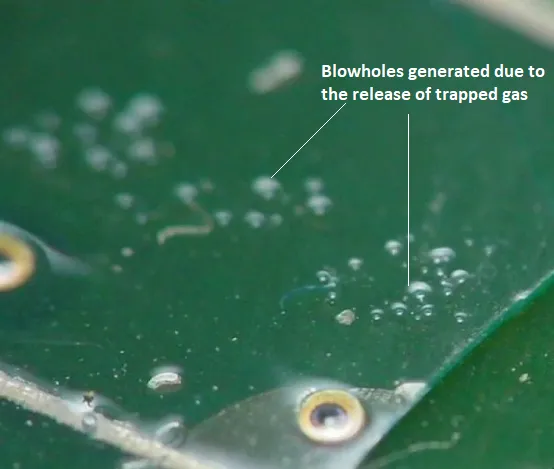
One of the leading causes of solder joint voids is solder paste outgassing. Solder paste, a mixture of flux and solder particles, releases gases during the reflow process as the flux activates and evaporates. If these gases get trapped within the molten solder, they form voids. This issue is particularly prominent in BGA assemblies because the solder balls are hidden beneath the component, limiting gas escape routes. Research indicates that improper stencil design or excessive solder paste volume can increase outgassing, leading to void percentages as high as 30-40% in some cases.
2. Inadequate Reflow Profiling
The reflow soldering process involves heating the PCB to melt the solder paste and form joints. If the reflow profile—temperature ramp-up, peak, and cooling phases—is not optimized, it can trap gases or cause uneven solder melting. For instance, a rapid temperature increase can lead to violent outgassing, while insufficient peak temperature may prevent full solder wetting, both contributing to voids. BGAs are especially sensitive to reflow profiles due to their complex thermal mass.
3. PCB and Component Surface Contamination
Contaminants like moisture, oxides, or residues on the PCB pads or component leads can interfere with solder wetting, creating gaps or voids. Moisture, in particular, can vaporize during reflow, forming bubbles within the solder joint. For BGA components, where solder balls are pre-applied, ensuring clean surfaces is crucial to prevent void formation.
4. Design and Material Issues
PCB design elements, such as pad size, via placement, and thermal relief patterns, can influence void formation. For example, vias-in-pad without proper filling can trap air, leading to voids during reflow. Additionally, the choice of solder paste and flux type can impact voiding. Some fluxes are more prone to outgassing, while certain solder alloys may not flow as effectively, increasing the risk of voids.
Detecting Solder Joint Voids: The Role of X-Ray Inspection
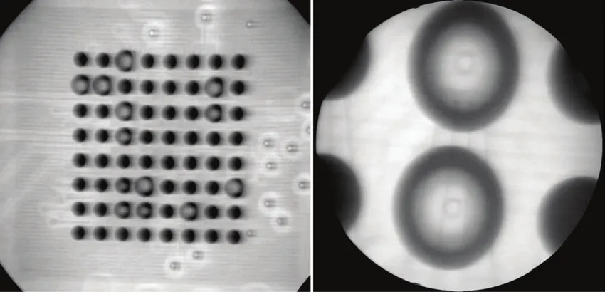
Detecting solder joint voids, especially in BGA components, is challenging because the solder connections are hidden beneath the package. Traditional visual inspection methods are ineffective, which is why X-ray inspection for solder voids has become an industry standard. Let’s explore how this technology works and why it’s essential.
How X-Ray Inspection Works
X-ray inspection uses high-resolution imaging to penetrate through the component and PCB layers, revealing the internal structure of solder joints. Voids appear as darker spots within the solder due to their lower density compared to the surrounding material. Modern X-ray systems can detect voids as small as 5% of the solder joint area, providing detailed insights into their size, location, and distribution.
Benefits of X-Ray Inspection for BGA Voids
For BGA components, X-ray inspection is indispensable. It allows manufacturers to assess the quality of hundreds of solder joints simultaneously without destructive testing. By identifying void percentages and patterns, engineers can correlate defects with specific process issues, such as solder paste outgassing or reflow profiling errors. Industry standards, like IPC-A-610, often specify acceptable void limits (typically below 25% for BGA joints), and X-ray inspection ensures compliance.
Limitations and Complementary Methods
While X-ray inspection is powerful, it’s not without limitations. It can be time-consuming for large batches, and interpreting the images requires skilled operators. In some cases, complementary methods like acoustic microscopy or destructive cross-sectioning are used to validate findings. However, for non-destructive, high-volume testing, X-ray remains the go-to solution.
Suggested Reading:BGA X-Ray Secrets: Detecting Hidden Solder Joint Issues for Enhanced Performance
Prevention Strategies for Solder Joint Voids
Preventing solder joint voids requires a multi-faceted approach, addressing everything from material selection to process optimization. Below are proven strategies, with a focus on techniques like reflow profiling for void reduction and vacuum reflow soldering.
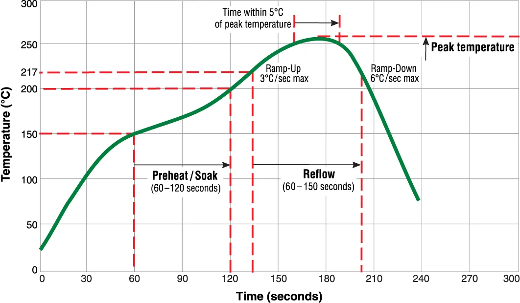
1. Optimize Reflow Profiling for Void Reduction
Creating an effective reflow profile is one of the most impactful ways to reduce voids. A well-designed profile ensures proper flux activation, gas release, and solder melting. Key considerations include:
- Preheat Phase: Gradually heat the board to 150-180°C over 60-90 seconds to activate flux and minimize rapid outgassing.
- Soak Phase: Maintain a temperature of 150-200°C for 60-120 seconds to allow gases to escape before the solder melts.
- Peak Phase: Reach a peak temperature of 235-245°C (depending on solder alloy) for 20-40 seconds to ensure complete melting without overheating.
- Cooling Phase: Cool at a controlled rate of 2-4°C per second to prevent thermal stress.
Testing different profiles and monitoring void levels via X-ray inspection can help fine-tune the process for specific BGA components or board designs.
2. Use Vacuum Reflow Soldering
Vacuum reflow soldering is an advanced technique that significantly reduces solder joint voids. By performing the reflow process in a vacuum chamber, the surrounding pressure is lowered, allowing trapped gases from solder paste outgassing to escape more easily. Studies have shown that vacuum reflow can reduce void percentages in BGA joints from 30% to under 10%, improving both mechanical and thermal performance. While this method requires specialized equipment and may increase production costs, it’s ideal for high-reliability applications.
3. Control Solder Paste Application
Proper solder paste application is critical to minimizing voids. Use a stencil design that matches the pad geometry and ensures uniform paste deposition. Avoid over-applying paste, as excess material can trap more gases during reflow. Additionally, choose a solder paste with low-voiding flux formulations, which are specifically designed to reduce outgassing. Storing solder paste at recommended temperatures (typically 2-10°C) and allowing it to reach room temperature before use can also prevent moisture absorption and subsequent voiding.
4. Improve PCB Design and Preparation
Design considerations play a big role in void prevention. For BGA components, use via-in-pad designs with proper plugging or capping to prevent air entrapment. Optimize pad sizes to balance solder volume and wetting. Before assembly, bake PCBs and components at 100-125°C for 4-8 hours to remove moisture, especially for moisture-sensitive devices. Clean surfaces to eliminate contaminants that could interfere with solder flow.
5. Monitor and Adjust Flux Activity
Flux is essential for removing oxides and promoting solder wetting, but its activity level must be balanced. Highly active fluxes can produce more gases, increasing void risk. Work with your solder paste supplier to select a formulation with moderate activity and low residue, tailored for BGA applications. Applying flux evenly and avoiding excess can further reduce void formation.
Practical Tips for Minimizing Solder Joint Voids
Beyond the major strategies, here are some additional tips to keep voiding in check during PCB assembly:
- Regularly calibrate reflow ovens to ensure consistent temperature profiles across the board.
- Use nitrogen atmosphere during reflow to reduce oxidation and improve solder wetting.
- Conduct periodic X-ray inspections on sample boards to catch void trends early.
- Train operators on proper handling and storage of materials to avoid contamination.
- Collaborate with material suppliers to test and validate low-voiding solder pastes for your specific applications.
The Impact of Solder Joint Voids on Reliability
Voiding isn’t just a cosmetic issue; it directly affects the performance and lifespan of electronic assemblies. In BGA components, voids can lead to poor heat dissipation, causing overheating in high-power applications. They can also create stress concentration points, increasing the risk of cracking under thermal cycling or mechanical shock. For critical industries like medical or aerospace, where failure rates must be near zero, controlling solder joint voids is non-negotiable. By implementing the strategies outlined above, you can achieve void levels well below the industry threshold of 25%, ensuring robust and reliable connections.
Conclusion: Building Stronger Solder Joints with ALLPCB
Solder joint voids, especially in BGA assemblies, pose a significant challenge in electronics manufacturing. From solder paste outgassing to improper reflow profiling, the causes are varied, but the solutions are within reach. By leveraging advanced detection methods like X-ray inspection for solder voids and adopting prevention techniques such as vacuum reflow soldering and optimized reflow profiling for void reduction, you can achieve high-quality, reliable solder joints.
At ALLPCB, we’re committed to supporting your success with cutting-edge assembly services and expert guidance. Whether you need assistance with process optimization or high-precision PCB manufacturing, our team is here to help you minimize solder joint voids and maximize product reliability. Trust us to be your partner in creating electronics that stand the test of time.


