 ALLPCB


Reflow soldering is a cornerstone of modern electronics manufacturing, enabling the precise and efficient assembly of surface-mount components onto printed circuit boards (PCBs). Whether you're a hobbyist building your first circuit or an engineer working on a high-volume production line, understanding reflow soldering is essential for creating reliable, high-performance electronics. In this guide, we break down the reflow soldering process, share practical tips for beginners, and highlight common pitfalls to avoid, ensuring your projects achieve strong, consistent solder joints.
What Is Reflow Soldering?
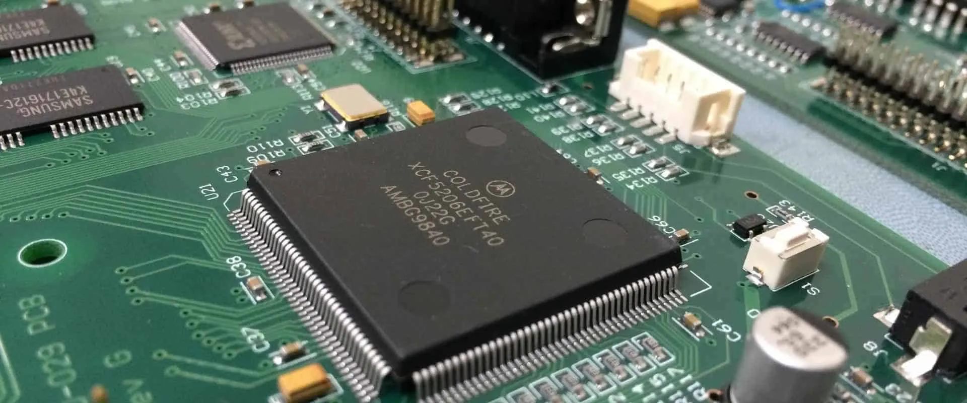
Reflow soldering is a process used to attach surface-mount technology (SMT) components to a PCB by applying solder paste, placing components, and heating the assembly in a controlled manner to melt the solder. Once cooled, the solder forms a permanent electrical and mechanical connection between the components and the PCB. This method is widely used in electronics manufacturing due to its ability to handle complex boards with high component density, making it ideal for devices like smartphones, laptops, and IoT gadgets.
Unlike wave soldering, which is suited for through-hole components, reflow soldering excels in SMT assembly because it allows multiple components to be soldered simultaneously. The process is highly automated, ensuring precision and repeatability, which is critical for both prototype development and large-scale production.
Why Reflow Soldering Matters for Engineers
For engineers, reflow soldering is more than just a manufacturing step - it's a critical process that impacts the reliability and performance of electronic devices. A well-executed reflow process ensures strong solder joints, minimizing issues like open circuits, tombstoning, or solder bridges that can lead to device failure. According to industry studies, poor solder joint quality accounts for up to 60% of PCB assembly defects, making mastery of reflow soldering a priority for producing robust electronics.
Reflow soldering also supports the trend toward miniaturization in electronics. As components shrink to sizes like 0201 (0.6mm x 0.3mm) and below, precise control over solder paste application and thermal profiles becomes essential to avoid defects and ensure functionality. By understanding reflow soldering, engineers can design PCBs that are optimized for manufacturability and performance.
The Reflow Soldering Process: Step-by-Step
The reflow soldering process consists of several distinct stages, each requiring careful attention to detail. Below, we outline the key steps to help beginners navigate the process effectively.
1. PCB Preparation and Solder Paste Application
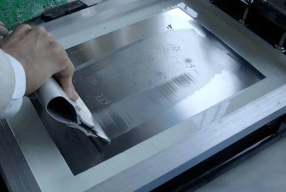
Before soldering begins, the PCB must be clean and free of contaminants like dust or oxidation, which can impair solder joint quality. Solder paste - a mixture of tiny solder particles, flux, and solvents - is applied to the PCB's contact pads using a stencil or screen-printing process. The stencil, typically made of stainless steel, ensures precise deposition of solder paste only where components will be placed.
For example, a typical solder paste for lead-free soldering might consist of a tin-silver-copper (SAC) alloy, such as SAC305 (96.5% tin, 3% silver, 0.5% copper), with a melting point around 217-220°C. The flux in the paste removes oxidation and enhances solder flow, ensuring a strong bond. Applying the right amount of paste is critical - too much can cause solder bridges, while too little may result in weak joints.
2. Component Placement
Once the solder paste is applied, electronic components such as resistors, capacitors, and integrated circuits are placed onto the PCB using a pick-and-place machine or, for hobbyists, tweezers. Alignment is crucial, as misaligned components can lead to defects like tombstoning, where a component lifts vertically due to uneven heating. Automated pick-and-place machines ensure repeatability, placing components with tolerances as tight as ±0.01mm in high-end systems.
For beginners working manually, using a magnifying glass or microscope can help ensure accurate placement. Components should sit flat on the solder paste, with leads or pads aligned with the PCB's contact points.
3. Reflow Oven Heating
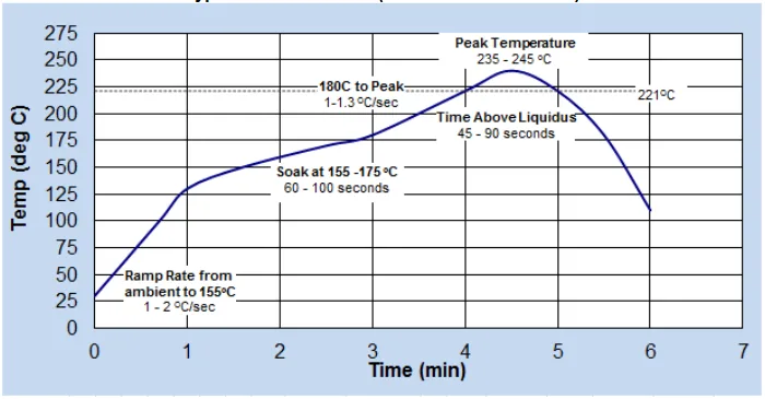
The heart of reflow soldering is the reflow oven, which heats the PCB assembly to melt the solder paste. The process follows a precise thermal profile with four main zones:
- Preheat Zone: Gradually raises the PCB temperature at a rate of 1-2°C per second to avoid thermal shock. This stage, typically lasting 60-120 seconds, also allows solvents in the solder paste to evaporate. Target temperature: 150-180°C.
- Soak Zone: Maintains a steady temperature (around 150-200°C for SAC alloys) for 60-90 seconds to ensure even heating across the board and activate the flux, which cleans the surfaces for soldering.
- Reflow Zone: Raises the temperature above the solder's melting point (e.g., 217°C for SAC305) to a peak of 235-250°C for 20-40 seconds. The solder melts, forming liquid joints that bond components to the PCB.
- Cooling Zone: Cools the assembly at a controlled rate of 2-4°C per second to solidify the solder joints without causing thermal stress. Rapid cooling can lead to brittle joints, while slow cooling may cause intermetallic growth, weakening the bond.
Hobbyists without access to a reflow oven can use a toaster oven or hot plate, though these lack the precise temperature control of industrial ovens. For example, a toaster oven may require manual monitoring to approximate the reflow profile, targeting a peak temperature of 240°C for lead-free solder.
Related Reading: Mastering the Reflow Soldering Temperature Profile: A Step-by-Step Guide
4. Inspection and Quality Control
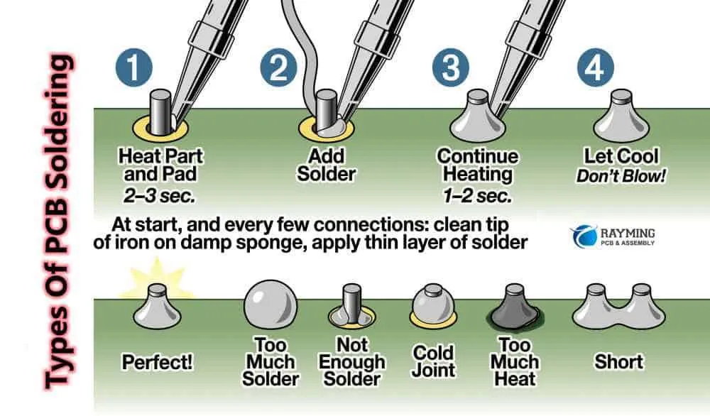
After cooling, the PCB is inspected to ensure solder joint quality. Visual inspection, often aided by a magnifying glass or automated optical inspection (AOI) systems, checks for defects like solder bridges, cold joints (dull, cracked joints), or tombstoning. For high-reliability applications, X-ray inspection may be used to detect hidden voids or incomplete solder flow.
A good solder joint is shiny, smooth, and cone-shaped, with no excess solder or cracks. For instance, a properly formed joint on a 0805 resistor (2mm x 1.25mm) should have a fillet height of approximately 0.2-0.5mm, ensuring a strong electrical connection.
Tips for Successful Reflow Soldering
To help beginners achieve reliable results, here are practical tips drawn from industry best practices:
- Choose the Right Solder Paste: Select a paste compatible with your components and PCB material. For lead-free soldering, SAC305 is a common choice due to its balance of cost, performance, and melting point (217°C). Check the paste's datasheet for recommended reflow profiles.
- Clean the PCB Thoroughly: Remove contaminants like dust or grease using isopropyl alcohol and a lint-free cloth to ensure proper solder adhesion.
- Use a Quality Stencil: A laser-cut stainless steel stencil with precise apertures (e.g., 0.1mm thickness for fine-pitch components) ensures consistent solder paste application.
- Monitor the Thermal Profile: Follow the solder paste manufacturer's recommended profile. For example, a soak time of 60-90 seconds at 150-200°C prevents uneven heating, reducing defects like tombstoning.
- Avoid Rapid Cooling: Cool the PCB at 2-4°C per second to prevent thermal shock, which can crack components or weaken joints.
- Inspect Every Joint: Use a magnifying glass or AOI to check for defects immediately after soldering. A solder joint with a contact angle of 30-45° is typically ideal for SMT components.
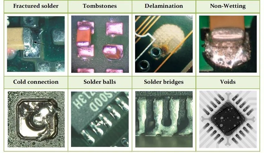
Common Reflow Soldering Problems and Solutions
Even with careful preparation, issues can arise during reflow soldering. Here are common problems and how to address them:
- Tombstoning: Occurs when a component lifts on one side, resembling a tombstone. Causes include uneven heating or excessive solder paste. Solution: Ensure uniform solder paste application and a balanced thermal profile. Place larger components symmetrically to minimize thermal gradients.
- Solder Bridges: Excess solder connects adjacent pads, causing shorts. Solution: Reduce solder paste volume by adjusting stencil aperture size (e.g., 90% of pad area for fine-pitch components) and verify stencil alignment.
- Cold Solder Joints: Dull, cracked joints indicate incomplete melting. Solution: Increase peak temperature (e.g., to 240°C for SAC305) or extend reflow time by 5-10 seconds, staying within component tolerances.
- Solder Balls: Small solder spheres form due to excess paste or poor stencil design. Solution: Optimize stencil apertures (e.g., 1:1 ratio with pad size) and ensure proper paste storage to prevent degradation.
How ALLPCB Supports Your Reflow Soldering Needs
For engineers seeking reliable PCB assembly, partnering with an experienced manufacturer can streamline the reflow soldering process. At ALLPCB, we offer advanced SMT assembly services, including quick-turn prototyping and high-volume production. Our state-of-the-art reflow ovens with 10 temperature zones ensure precise thermal profiles, minimizing defects like tombstoning or solder bridges. With global logistics and a robust supply chain, we source high-quality components and solder pastes, such as SAC305, tailored to your project's needs. Whether you're prototyping a new design or scaling production, our expertise ensures your PCBs meet stringent quality standards.
Conclusion
Reflow soldering is a powerful technique that enables engineers to build reliable, high-performance electronics. By understanding the process - preparing the PCB, applying solder paste, placing components, and controlling the thermal profile - you can achieve strong, consistent solder joints. For beginners, mastering reflow soldering requires attention to detail, the right tools, and awareness of common pitfalls. With practice and the right resources, you'll be well-equipped to tackle SMT assembly projects with confidence.
Whether you're a hobbyist experimenting in a garage or an engineer designing cutting-edge devices, reflow soldering is a skill worth mastering. Start with small projects, refine your technique, and consider partnering with a trusted manufacturer like ALLPCB to bring your PCB design to life with precision and efficiency.


