 ALLPCB


If you're looking to understand how wave soldering works for through-hole components in mass production, you've come to the right place. Wave soldering is a widely used method in PCB assembly, especially for through-hole components, where efficiency and reliability are key. In this blog, we'll dive into the essentials of wave soldering machine use for PCB assembly, the molten solder wave process, fluxing methods for PCB soldering, and tips for optimizing conveyor speed in wave soldering. We'll break down each step to help you achieve high-quality results in your production line.
Whether you're an engineer, a production manager, or a hobbyist scaling up to mass production, this guide will walk you through the ins and outs of wave soldering for through-hole component PCB assembly. Let's explore this powerful technique to ensure strong, consistent solder joints for your projects.
What is Wave Soldering and Why Use It for Through-Hole Components?
Wave soldering is a bulk soldering process used primarily for assembling printed circuit boards (PCBs) with through-hole components. Unlike surface mount technology (SMT), where components sit on the board's surface, through-hole components have leads that pass through holes in the PCB and are soldered on the opposite side. Wave soldering is ideal for this setup because it allows for quick, automated soldering of multiple joints at once.
In mass production, efficiency matters. Wave soldering machines streamline the process by passing PCBs over a wave of molten solder, which creates strong electrical and mechanical connections between the component leads and the board. This method is particularly effective for larger components, high-power devices, and connectors that require robust soldering, making it a go-to choice for many industries despite the rise of SMT.
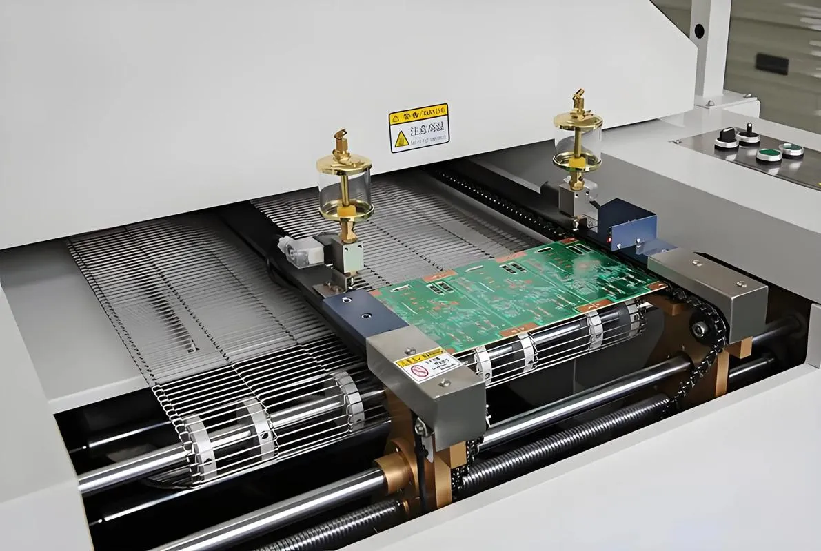
How Does the Molten Solder Wave Process Work?
The molten solder wave process is the heart of wave soldering. Here's a step-by-step look at how it works in PCB assembly:
- Flux Application: Before soldering, a layer of flux is applied to the underside of the PCB. Flux cleans the metal surfaces by removing oxides and impurities, ensuring the solder adheres properly to the component leads and pads.
- Preheating: The PCB is preheated to a temperature typically between 100°C and 150°C. This step reduces thermal shock when the board contacts the hot solder wave and activates the flux for better performance.
- Solder Wave Contact: The PCB moves over a wave of molten solder, usually a tin-lead alloy or lead-free solder, maintained at around 250°C to 260°C. The wave wets the exposed metal areas, forming solid joints as the solder cools.
- Cooling: After passing over the wave, the PCB cools down, solidifying the solder joints. This step is critical to avoid defects like cold solder joints or thermal stress.
The molten solder wave process is highly efficient for through-hole component PCB assembly because it solders multiple connections simultaneously. However, precise control of temperature and wave height is essential to prevent issues like bridging (solder connecting adjacent pins) or insufficient wetting.
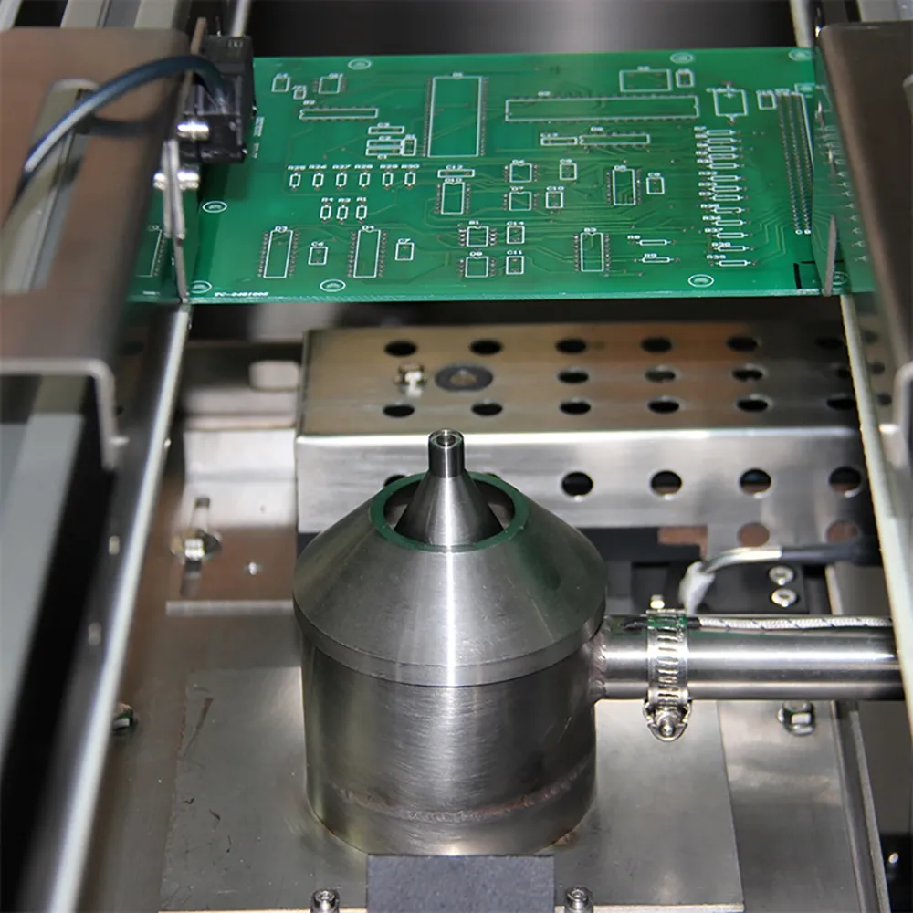
Fluxing Methods in PCB Soldering: Getting It Right
Fluxing is a crucial step in wave soldering, as it directly impacts the quality of the solder joints. There are two primary fluxing methods used in PCB soldering during wave soldering:
- Spray Fluxing: A fine mist of flux is sprayed onto the underside of the PCB. This method offers uniform coverage and is adjustable to match the board's design. It's ideal for high-speed production lines as it minimizes flux waste.
- Foam Fluxing: The PCB passes over a foam of flux created by bubbling air through a liquid flux reservoir. This older method is less precise but still effective for simpler designs or when cost is a concern.
Choosing the right fluxing method for PCB soldering depends on your production needs. For intricate boards with dense component layouts, spray fluxing provides better control. Additionally, the type of flux—rosin-based, water-soluble, or no-clean—should match the PCB material and environmental regulations. For instance, no-clean flux reduces post-soldering cleaning but may leave residues that affect long-term reliability if not managed properly.
Proper flux application prevents defects like solder balls or poor wetting, ensuring reliable connections for through-hole components. Always monitor flux coverage and adjust application settings to avoid over- or under-fluxing, which can lead to production delays or rework.
Optimizing Conveyor Speed in Wave Soldering for Best Results
Conveyor speed is a critical parameter in wave soldering that directly affects the quality of solder joints and overall production efficiency. Optimizing conveyor speed in wave soldering requires balancing speed with exposure time to the solder wave. Here's how to approach it:
- Too Fast: If the conveyor moves too quickly, the PCB may not spend enough time in contact with the molten solder wave. This can result in incomplete soldering, cold joints, or weak connections. Typical speeds for wave soldering range from 0.5 to 2 meters per minute, but this varies based on board size and complexity.
- Too Slow: Conversely, a slow conveyor speed can overexpose the PCB to heat, risking component damage or excessive solder buildup, which may cause bridging between pins.
- Finding the Sweet Spot: Test different speeds during setup to find the optimal rate. For most standard through-hole component PCB assemblies, a speed of around 1.2 to 1.5 meters per minute provides adequate solder contact time—typically 2 to 4 seconds—while preventing thermal stress.
Other factors, like preheat temperature and solder wave height, also interact with conveyor speed. For example, a higher preheat temperature (closer to 150°C) may allow for a slightly faster conveyor speed since the board is already closer to soldering temperature. Regularly monitor and adjust these settings based on defect rates and joint quality during production runs.
Benefits and Challenges of Wave Soldering in Mass Production
Wave soldering offers several advantages for mass production of through-hole component PCB assembly, but it also comes with challenges. Understanding both helps in making informed decisions for your production line.
Benefits:
- High Throughput: Wave soldering machines can process hundreds of boards per hour, making them ideal for large-scale manufacturing.
- Cost-Effective: Compared to manual soldering, wave soldering reduces labor costs and ensures consistent results across batches.
- Reliability: Properly executed wave soldering creates strong, durable joints suitable for high-power and mechanical stress applications.
Challenges:
- Design Limitations: Wave soldering is less suited for mixed-technology boards with both through-hole and surface-mount components, as SMT parts may not withstand the process.
- Thermal Stress: Excessive heat from the solder wave can damage sensitive components if preheating and cooling aren't managed well.
- Defect Risks: Issues like solder bridging, insufficient wetting, or excess flux residue can occur if parameters like conveyor speed or wave height aren't optimized.
By addressing these challenges through careful process control and regular maintenance of wave soldering equipment, manufacturers can maximize the benefits of this method in mass production.
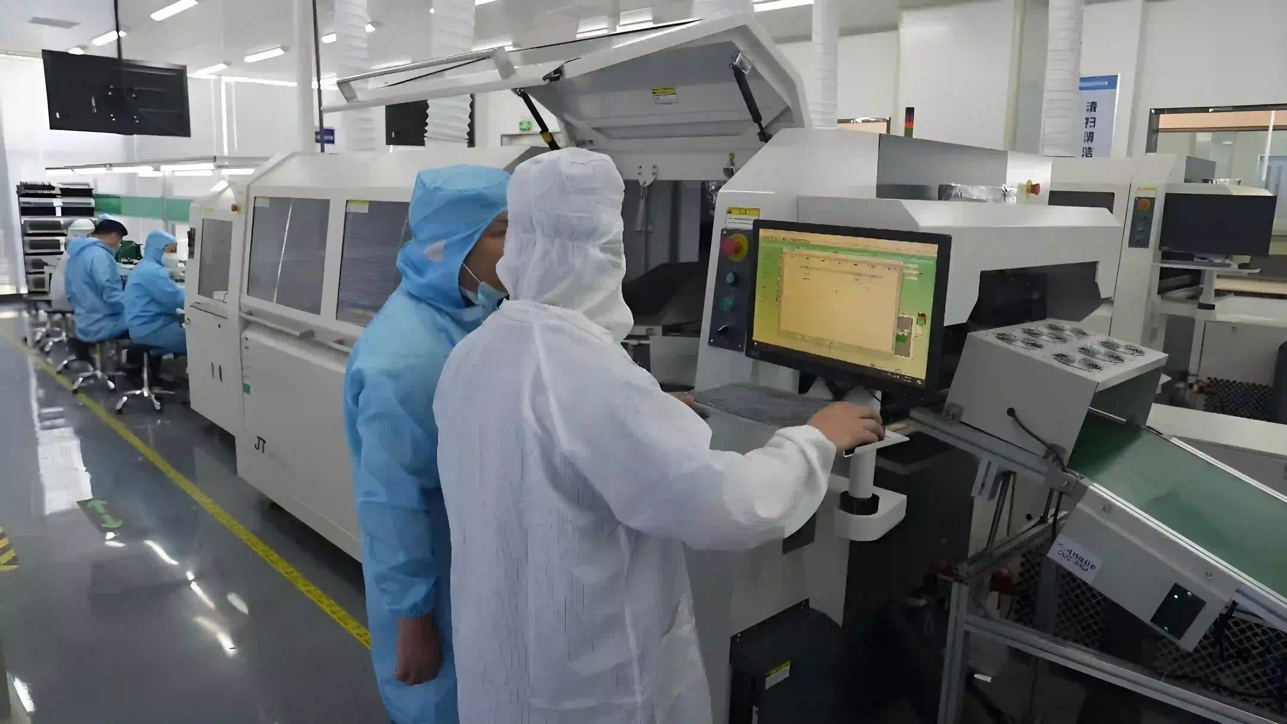
Best Practices for Wave Soldering Machine Use in PCB Assembly
To ensure success when using a wave soldering machine for PCB assembly, follow these best practices tailored for through-hole components:
- Board Design Optimization: Design your PCB with wave soldering in mind. Orient components to minimize shadowing (where leads block solder flow) and space pins adequately to avoid bridging. A minimum pin spacing of 2.54 mm is often recommended for standard through-hole components.
- Solder Alloy Selection: Choose the right solder alloy based on your application. Lead-free solders, like SAC305 (Sn96.5Ag3.0Cu0.5), are common for compliance with environmental standards, but they require higher temperatures (around 260°C) compared to traditional tin-lead solders (around 250°C).
- Regular Maintenance: Keep the wave soldering machine in top condition by cleaning the solder pot to remove dross (oxidized solder) and checking the wave height for consistency. Dross buildup can contaminate the solder wave, leading to poor joints.
- Quality Control: Inspect solder joints post-process using automated optical inspection (AOI) or manual checks. Look for issues like incomplete fillets, solder balls, or bridging, and adjust process parameters as needed.
Implementing these practices can significantly improve the quality and efficiency of your wave soldering process, ensuring reliable results in mass production.
Conclusion: Mastering Wave Soldering for Through-Hole PCB Assembly
Wave soldering remains a cornerstone of PCB assembly for through-hole components, especially in mass production where speed and reliability are paramount. By understanding the molten solder wave process, mastering fluxing methods for PCB soldering, and optimizing conveyor speed in wave soldering, you can achieve consistent, high-quality results. The key lies in balancing process parameters, maintaining equipment, and adhering to best practices tailored to your specific production needs.


