 ALLPCB


In the fast-paced world of electronics, improving electrical performance is a top priority for engineers and manufacturers. Whether you're designing high-speed data systems or compact consumer devices, the quality of connector PCB plating, especially the gold plating process, plays a critical role. Issues like poor gold layer adhesion, inconsistent gold-plated holes, or quality problems in volume connectors can lead to signal loss, increased impedance, or even device failure. So, how can you ensure optimal performance? The answer lies in mastering the gold plating process, addressing common quality challenges, and adopting best practices for connector PCB design and manufacturing.
In this comprehensive guide, we'll dive deep into the factors that impact electrical performance in connector PCBs. We'll explore the gold plating process, common quality problems with gold-plated holes and layers, and actionable strategies to enhance performance for volume connectors. Let's get started with everything you need to know to achieve reliable, high-quality results.
Why Electrical Performance Matters in Connector PCBs
Connector PCBs are the backbone of many electronic systems, enabling seamless communication between components. From smartphones to industrial machinery, these connectors must handle high-speed signals, maintain low impedance, and resist wear over time. Poor electrical performance can result in signal degradation, higher resistance, and unreliable connections, leading to costly failures or reduced product lifespan.
The gold plating process is often used in connector PCBs due to its excellent conductivity and corrosion resistance. A well-executed gold layer ensures minimal signal loss (often below 0.1 ohms of contact resistance) and durability for thousands of mating cycles (up to 10,000 in some high-end applications). However, achieving this level of performance requires precision in manufacturing and attention to potential quality problems.
Understanding the Gold Plating Process for Connector PCBs
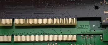
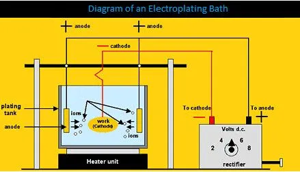
The gold plating process is a critical step in manufacturing connector PCBs, as it directly impacts electrical performance. Gold is applied as a thin layer over a base metal, typically nickel, to provide a conductive, corrosion-resistant surface. There are two main methods used in the industry: electroplating and immersion gold (ENIG).
- Electroplating: This method uses an electric current to deposit a gold layer onto the connector surface. It allows for thicker coatings (often 30-50 microinches) and is ideal for high-wear applications like edge connectors.
- Immersion Gold (ENIG): A chemical process that deposits a thinner gold layer (typically 2-5 microinches) over nickel. It's widely used for its uniform coverage and suitability for fine-pitch components.
Both methods aim to create a gold layer that enhances conductivity and protects against oxidation. However, the thickness and quality of this layer can vary, affecting electrical performance. For instance, a gold layer that's too thin may wear out quickly, while an overly thick layer can increase manufacturing costs without significant benefits.
Common Quality Problems in Gold-Plated Holes and Layers
While gold plating offers many advantages, quality problems can arise during the manufacturing of connector PCBs, especially in high-volume production. These issues can compromise electrical performance and lead to failures in the field. Below are some of the most common challenges with gold-plated holes and layers, along with their potential impact.
1. Poor Adhesion of the Gold Layer
If the gold layer doesn't bond properly to the underlying nickel or copper, it can peel or flake off over time. This often happens due to inadequate surface preparation or contamination during plating. Poor adhesion increases contact resistance (sometimes exceeding 1 ohm) and can cause intermittent connections.
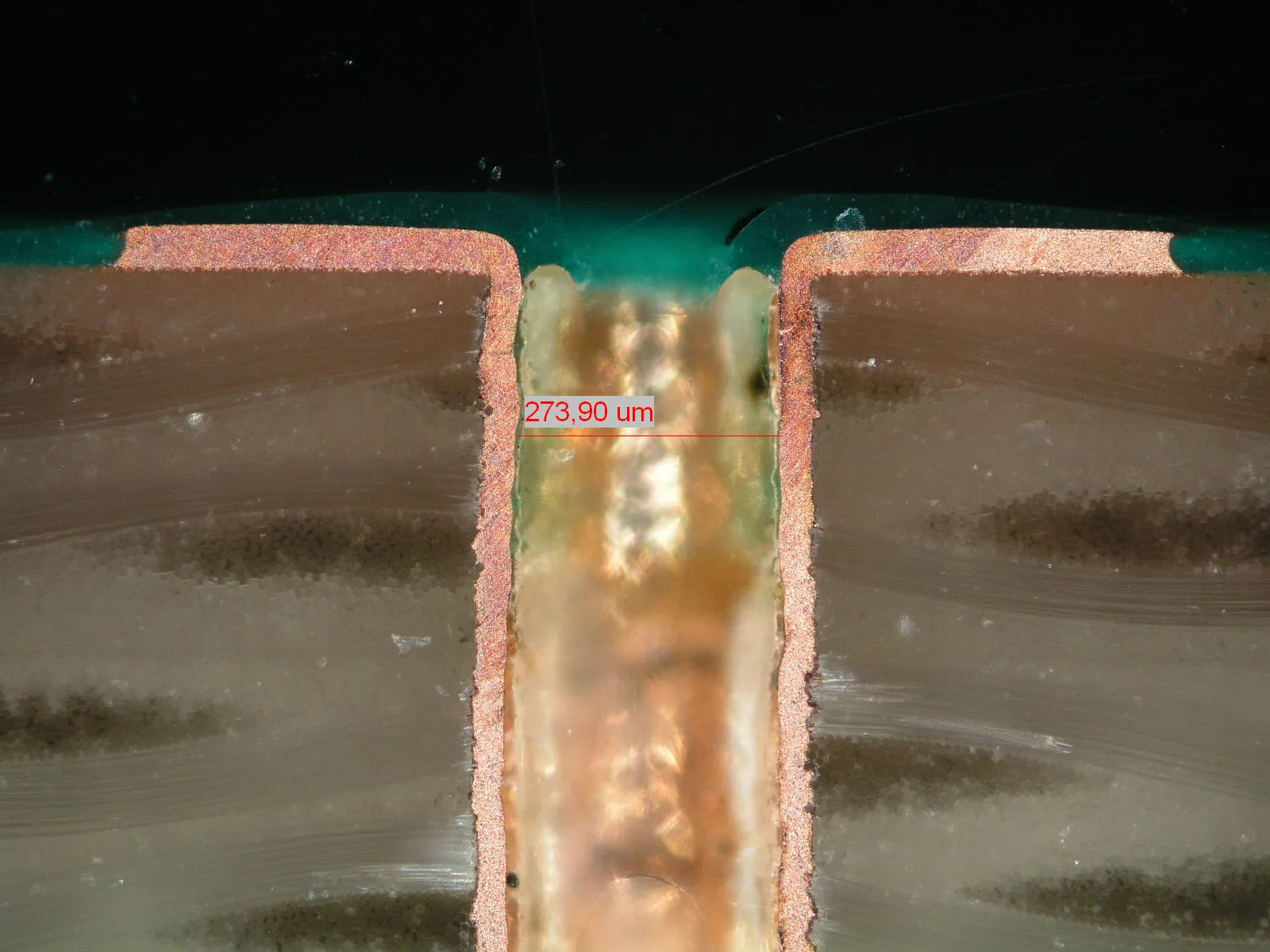
2. Inconsistent Gold Thickness in Holes
Gold-plated holes, often used in pin connectors, are prone to uneven plating. In high-aspect-ratio holes, the gold layer may be thinner at the bottom, leading to higher resistance or corrosion over time. This is a significant concern for volume connectors, where hundreds of holes must be plated uniformly.
3. Porosity in the Gold Layer
A porous gold layer allows moisture or contaminants to reach the base metal, causing corrosion and degrading performance. Porosity often results from improper plating parameters, such as incorrect current density or bath composition, and can reduce the lifespan of connectors to under 1,000 mating cycles.
4. Gold Embrittlement in Soldering
During soldering, gold can dissolve into the solder joint, forming brittle intermetallic compounds. If the gold content in the joint exceeds 3-5% by weight, it can lead to cracking under stress, compromising reliability. This is a critical issue for connectors mounted on PCBs.
Strategies for Improving Electrical Performance in Connector PCBs
Addressing quality problems in the gold plating process and connector design is essential for optimizing electrical performance. Here are actionable strategies to enhance the reliability and efficiency of connector PCBs, especially for volume production.
1. Optimize the Gold Plating Process
Control over plating parameters is key to achieving a consistent gold layer. Manufacturers should monitor bath chemistry, current density, and plating time to ensure uniform thickness (targeting 30 microinches for electroplating in high-wear areas). Regular testing, such as X-ray fluorescence (XRF) for thickness measurement, can help detect variations early.
Additionally, proper surface preparation—such as thorough cleaning and activation of the base metal—ensures strong adhesion of the gold layer. This step can reduce failure rates by up to 40% in high-volume connector production.
2. Use Selective Plating for Cost and Quality
For connectors with specific high-contact areas, selective gold plating can be a game-changer. By applying gold only where it's needed (e.g., contact points), manufacturers can reduce costs while maintaining performance. This approach is particularly effective for volume connectors, where material savings add up quickly.
3. Improve Gold-Plated Hole Quality
For gold-plated holes, adopting advanced plating techniques like pulse plating can improve uniformity. Pulse plating alternates current on and off, allowing better gold distribution in deep holes. This can reduce resistance variations by up to 20% in high-aspect-ratio vias, ensuring consistent performance across all connections.
4. Mitigate Gold Embrittlement Risks
To prevent embrittlement during soldering, consider using a nickel barrier layer of at least 50 microinches between the gold and solder. This limits gold dissolution into the solder joint. Additionally, using low-gold-content plating (e.g., immersion gold with minimal thickness) can further reduce risks in applications where soldering is required.
5. Test and Validate Connector Performance
Rigorous testing is essential to identify quality problems before connectors reach the market. Electrical testing for contact resistance (targeting below 0.05 ohms), environmental testing for corrosion resistance (e.g., salt spray tests), and mechanical testing for mating durability (minimum 5,000 cycles) can ensure that connectors meet performance standards.
Designing Connector PCBs for Volume Production
In high-volume connector manufacturing, balancing cost, quality, and performance is a challenge. Here are some design considerations to optimize electrical performance while maintaining scalability.
- Material Selection: Choose base materials with low dielectric loss for high-speed applications (e.g., FR-4 with a dielectric constant below 4.0). Pair this with a reliable gold plating process to minimize signal loss.
- Trace and Via Design: Minimize impedance mismatches by designing traces with controlled widths (e.g., 50 ohms for standard high-speed signals) and using properly plated vias. Poorly plated vias can increase signal reflection by up to 10%.
- Connector Layout: Position connectors to reduce crosstalk, spacing signal lines at least 3x the trace width apart. This can lower interference in densely packed volume connectors.
By integrating these design principles with a robust gold plating process, manufacturers can achieve consistent electrical performance even in large-scale production runs.
The Future of Connector PCB Plating and Performance
As electronics continue to evolve, the demand for faster, smaller, and more reliable connectors grows. Innovations in plating technology, such as nanotechnology-based gold coatings, promise even thinner yet more durable layers, potentially reducing contact resistance below 0.01 ohms. Additionally, automation in the gold plating process is improving precision, addressing quality problems in volume connectors by ensuring repeatability across millions of units.
Staying ahead of these trends means adopting cutting-edge practices today. By focusing on quality control, advanced testing, and optimized design, manufacturers can prepare for the next generation of high-performance electronics.
Conclusion: Achieving Excellence in Electrical Performance
Improving electrical performance in connector PCBs is a multifaceted challenge that hinges on the quality of the gold plating process. From addressing common quality problems like poor adhesion and uneven gold-plated holes to optimizing designs for volume connectors, every step matters. By implementing strict process controls, leveraging selective plating, and conducting thorough testing, manufacturers can ensure a reliable gold layer that delivers low resistance, high durability, and consistent performance.
Whether you're an engineer designing the next big device or a manufacturer scaling up production, focusing on these strategies will help you overcome quality challenges and meet the demands of modern electronics. With the right approach, your connector PCBs can achieve the electrical performance needed to power innovation.


