ALLPCB


Introduction
Flexible PCB design has become essential in modern electronics, particularly for wearable electronics where compact form factors and mechanical flexibility are paramount. Stacked vias in flex PCBs enable high-density interconnects by vertically aligning multiple vias through several layers, maximizing routing efficiency in limited spaces. However, integrating stacked vias into flex PCBs introduces unique challenges due to the dynamic bending and flexing motions these boards endure. PCB reliability becomes a critical concern, as failures in stacked vias can lead to open circuits or intermittent connections during repeated flex cycles. This article explores the engineering principles behind these challenges and provides structured solutions grounded in established design practices. Electrical engineers designing for applications like fitness trackers or medical wearables must balance density with long-term durability.
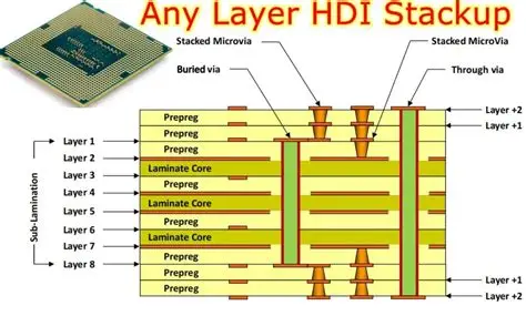
What Are Stacked Vias in Flex PCBs?
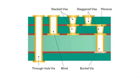
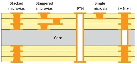
Stacked vias consist of multiple vias positioned directly atop one another, spanning several dielectric layers in a PCB stackup to create a continuous vertical interconnection. In flex PCBs, these structures typically traverse polyimide substrates or adhesive layers between copper foils, often formed using laser-drilled microvias followed by electroplating. Unlike through-holes, stacked vias minimize board real estate usage, making them ideal for high-density interconnect (HDI) flex designs. The process involves sequential buildup, where each via level is filled or plated to support the next, ensuring electrical continuity. However, the flexible nature of the base materials complicates fabrication and performance compared to rigid boards. Understanding this structure is key to appreciating why stacked vias in flex PCBs demand specialized design considerations.
Why Stacked Vias Matter in Flexible PCB Design
In wearable electronics, flex PCBs must conform to curved surfaces and withstand thousands of bend cycles, amplifying the need for reliable high-density routing. Stacked vias allow engineers to achieve finer pitch interconnects without expanding the overall footprint, supporting advanced features like integrated sensors and processors. PCB bending introduces strain that rigid vias cannot tolerate, making stacked configurations a double-edged sword: they enable density but heighten failure risks. Poor via reliability can cascade into system-level issues, such as signal loss or power delivery failures during motion. As devices shrink, the pressure to incorporate stacked vias grows, yet PCB reliability remains non-negotiable for user safety and product longevity. Engineers must weigh these trade-offs early in the flexible PCB design phase.
Key Challenges in Implementing Stacked Vias in Flex PCBs
The primary challenge stems from mechanical stresses during PCB bending, where outer layers experience tensile forces and inner layers compressive ones, concentrating strain at via barrels and interfaces. Stacked vias exacerbate this, as each level acts as a stress riser, promoting fatigue cracking in the copper plating or dielectric over repeated flexures. Thermal cycling compounds the issue through coefficient of thermal expansion (CTE) mismatches between copper and flexible dielectrics like polyimide, leading to delamination or void formation at via landings. Manufacturing difficulties, such as achieving uniform plating in narrow stacked structures, introduce defects like plating voids or barrel cracks that propagate under flex. These factors collectively undermine PCB reliability in dynamic applications. Designers often overlook bend radius limits, resulting in accelerated wear.
Technical Mechanisms Driving Via Failures
During PCB bending, the neutral axis shifts, causing vias near bend zones to endure shear and peel stresses proportional to their distance from the axis. Stacked vias, with their vertical column of interconnects, amplify cumulative strain, as misalignment between levels induces microcracks that grow with cycles. Electromigration accelerates under combined thermal and mechanical loads, particularly in high-current paths common in wearables. Dielectric cracking around via perimeters occurs when bend radii fall below material limits, severing connections. IPC-2223 provides guidelines on avoiding vias in high-flex regions to mitigate these mechanisms. [1][2] Finite element analysis reveals that stacked configurations double stress concentrations compared to staggered alternatives. Engineers can model these effects to predict cycle life accurately.
Practical Solutions and Best Practices for Reliable Stacked Vias
Position stacked vias exclusively in rigid or static flex zones, transitioning to fanout traces in bend areas to distribute stress. Opt for staggered vias, where each level offsets horizontally, reducing vertical stress stacking and improving thermal cycle endurance. Adhere to conservative aspect ratios (under 1:1 for microvias) and minimum annular ring sizes per IPC-2223 to enhance plating uniformity and crack resistance. Copper-fill vias before stacking to provide mechanical reinforcement and planar surfaces for subsequent layers. Select low-CTE polyimides and controlled copper weights to minimize mismatch during reflow or operation. Simulate bending with tools accounting for material anisotropy, validating designs against qualification tests like those in IPC-6013.
Related Reading: Stacked Via Reliability: Ensuring Robust Performance in Demanding PCB Applications
Advanced Strategies for Enhanced PCB Reliability
Incorporate tear-drop shaped pads at via landings to relieve stress concentrations and prevent cracking at corners. Limit stacking to two levels maximum, staggering subsequent vias to avoid excessive column height, which heightens reliability risks. Perform iterative reliability modeling incorporating bend radius, cycle count, and temperature excursions. Hybrid rigid-flex designs isolate stacked vias in rigid sections, using flex extensions for motion. Qualification via IPC-6013 bend and thermal shock tests ensures compliance before production. These practices extend mean time to failure significantly in wearable applications.
Related Reading: Laser Drilling for Flexible PCBs: Achieving High Density and Reliability
Troubleshooting Common Stacked Via Issues in Flex Designs
Engineers often encounter intermittent opens traced to via cracking; cross-section analysis reveals plating defects from poor sequential buildup. Delamination signals CTE issues, resolved by matching layer materials closely. If simulations predict failure, iterate to larger diameters or filled vias. Post-fabrication, inspect with X-ray for voids. Field returns from wearables highlight bend zone misuse, underscoring the need for zone-specific rules. Logical root-cause analysis, paired with standards adherence, resolves most issues efficiently.
Conclusion
Stacked vias enable dense flexible PCB designs vital for wearable electronics, yet PCB bending and thermal stresses pose significant reliability hurdles. By understanding failure mechanisms like strain concentration and plating defects, engineers can implement targeted solutions such as staggering, filling, and zonal placement. Adhering to IPC guidelines ensures robust performance under real-world flex cycles. Proactive simulation and testing mitigate risks, delivering durable interconnects. Ultimately, thoughtful flexible PCB design balances density with longevity, driving innovation in compact devices.
FAQs
Q1: Can stacked vias be reliably used in flex PCB designs for wearable electronics?
A1: Stacked vias suit flex PCBs in static zones but require careful placement away from bend areas to maintain PCB reliability. Stagger them or limit to two levels to reduce stress accumulation during bending. Follow IPC-2223 for via positioning and sizing to avoid cracking. This approach supports high-density needs without compromising flex life.
Q2: What are the main challenges with stacked vias in flex PCBs during PCB bending?
A2: PCB bending induces tensile and shear stresses on stacked vias, leading to copper fatigue and dielectric cracks over cycles. Stacked structures concentrate forces vertically, worsening reliability compared to staggered vias. Manufacturing plating issues like voids accelerate failures. Mitigate by using larger diameters and simulations.
Q3: How does IPC-6013 address stacked via reliability in flexible PCB design?
A3: IPC-6013 outlines qualification tests for flex PCBs, including bend cycling and thermal shock to verify via integrity. It ensures stacked vias withstand mechanical and environmental stresses in applications like wearables. Designers validate stackups against these criteria for production readiness.
Q4: What best practices improve stacked vias in flex PCB reliability?
A4: Avoid dynamic bend zones, prefer copper-filled vias, and stagger configurations for better strain distribution. Select low-CTE materials and adhere to aspect ratio limits. Reliability testing per standards confirms performance under flex conditions.