ALLPCB


Introduction
In high-speed PCB designs, maintaining precise signal integrity demands careful attention to impedance control during fabrication. Engineers often face challenges when communicating PCB impedance specifications to manufacturers, leading to potential mismatches that degrade performance. This article outlines a structured approach to defining impedance control PCB fabrication requirements, ensuring alignment between design intent and manufacturing capabilities. By providing clear PCB stackup specifications and impedance tables, designers can minimize iterations and achieve reliable outcomes. Understanding these processes empowers electrical engineers to specify requirements effectively, reducing risks in controlled impedance environments. The guidance here draws from established engineering practices to support robust signal transmission.
What Is Impedance Control and Why It Matters
Impedance control refers to the process of designing and fabricating PCB traces to maintain a consistent characteristic impedance along their length, crucial for high-frequency signals. Without proper control, signal reflections occur due to impedance discontinuities, causing crosstalk, attenuation, and timing errors in circuits like RF modules or data buses. In modern applications such as 5G communications and high-speed interfaces, impedance mismatches can lead to compliance failures and system instability. Manufacturers rely on precise PCB impedance specifications to adjust trace geometries during production, ensuring the final board meets design goals. This control becomes essential as signal speeds exceed gigahertz ranges, where even small variations in dielectric properties impact performance. Adhering to standards like IPC-2141A helps standardize these requirements across the supply chain.
Technical Principles of Impedance in PCBs
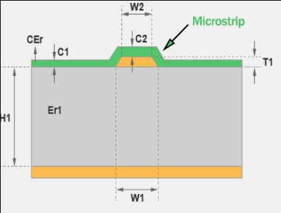
Characteristic impedance in PCBs arises from the interaction between trace geometry, dielectric materials, and surrounding ground planes. For microstrip lines on outer layers, impedance depends on trace width, copper thickness, and the effective dielectric constant of the substrate above and below the trace. Stripline configurations, embedded between planes, require consideration of dielectric thicknesses on both sides, making stackup symmetry critical. The formula for impedance incorporates factors like relative permittivity (Er), which varies with frequency and material composition. Engineers must account for manufacturing tolerances in copper etching and lamination, as these directly influence final impedance values. Accurate modeling using field solvers precedes fabrication to predict behaviors under real conditions.
Dielectric materials play a pivotal role, with low-loss variants offering stable Er for high-speed applications. Variations in glass weave orientation can cause impedance skew across the board, necessitating tight control in stackup design. Copper weight, typically expressed in ounces per square foot, affects trace resistance and skin effect at high frequencies. Reference planes provide return paths, and their proximity to signal traces defines coupling capacitance. These principles guide the creation of impedance tables that correlate trace dimensions to target values. Proper specification prevents deviations that compromise signal integrity.
Key Factors Influencing Impedance During Fabrication
Fabrication processes introduce variables that alter designed impedances, such as plating thickness buildup and dielectric compression during lamination. Etch tolerances, often in the range of microns, directly impact trace width, a primary impedance determinant. Material selection influences Er stability, with resin content and filler types affecting uniformity. Temperature and humidity during pressing can cause resin flow, altering layer thicknesses. Engineers must communicate these sensitivities through detailed PCB stackup specifications to enable manufacturer adjustments. Cross-section analysis post-lamination verifies actual dimensions against targets.
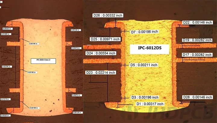
Ground plane discontinuities, vias, and bends also disrupt impedance continuity, requiring length-matched routing for differential pairs. For differential signaling, intra-pair spacing and gap to reference planes must align with common-mode and differential-mode targets. Manufacturing capabilities vary, so specifying test methods like time-domain reflectometry (TDR) ensures verification. Coupons on the panel edge allow non-destructive measurements without risking production boards. These factors underscore the need for collaborative specification to bridge design and fabrication.
Related Reading: Signal Layer Impedance Control: Achieving Optimal Signal Integrity in PCBs
Best Practices for PCB Impedance Specification
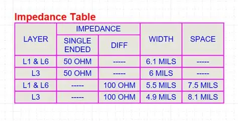
Start by developing a comprehensive stackup diagram that details layer count, material types, core and prepreg thicknesses, and copper weights. Include Er values for each dielectric, frequency of interest, and any symmetry requirements. For layers needing control, list target impedances, such as 50 ohms single-ended or 100 ohms differential, along with tolerances. Provide an impedance table PCB format outlining nominal trace widths, spacings, and corresponding Z values based on your calculations. This table serves as a reference for the manufacturer to fine-tune during engineering review. Clearly mark net classes or specific nets requiring control to avoid over-specification.
Communicate PCB manufacturer impedance requirements through fabrication drawings and notes. Specify measurement locations, such as multiple coupons per panel, and preferred test equipment standards. Request a pre-production stackup proposal from the manufacturer, including their material data sheets for validation. Iterate on trace widths if their models differ from yours, prioritizing TDR-verified data. For complex stackups, indicate via stub lengths or back-drilling needs to maintain impedance. These steps ensure impedance control PCB fabrication aligns with design margins.
Related Reading: The Ultimate Guide to Stackup Materials for Impedance Control in High Speed PCBs
Use standardized documentation to minimize ambiguity. Include a dedicated impedance control section in the manufacturing package, referencing applicable guidelines. For multilayer boards, specify reference plane assignments explicitly. If tighter tolerances are needed, justify with signal speed requirements and confirm manufacturer capabilities upfront. Post-fabrication, review test reports for compliance before assembly. This systematic approach enhances yield and performance.
- L2 — Microstrip — 50 ohms single-ended ±10%; Reference Plane: L1 Ground; Notes: High-speed signals
- L4 — Stripline — 100 ohms differential ±10%; Reference Plane: L3 & L5 Planes; Notes: USB pairs
- L6 — Microstrip — 50 ohms single-ended ±10%; Reference Plane: L7 Ground; Notes: Clock lines
Common Challenges and Troubleshooting in Impedance Specification
Mismatched expectations often arise from incomplete stackup details, leading to wider-than-expected trace etches. If manufacturer TDR shows deviations, check for Er discrepancies in their material database versus your assumptions. Asymmetric stackups exacerbate inner layer imbalances, so prioritize balanced constructions where possible. Vias transitioning layers introduce stubs; specify back-drilling or blind vias in requirements. Review panel utilization, as edge effects on coupons may not represent inner board regions accurately. Addressing these proactively through clear PCB impedance specification prevents costly respins.
In high-density designs, routing density limits width adjustments, forcing trade-offs with spacing rules. Collaborate early to assess feasibility, providing multiple width options per target Z. Frequency-dependent Er requires specifying the test frequency matching your operating band. For flex-rigid boards, hybrid stackups demand segmented specifications. Standards like IPC-6012E provide qualification criteria for verifying controlled impedance boards. Systematic troubleshooting maintains integrity across the process.
Conclusion
Specifying impedance control requirements demands precision in stackup documentation, target values, and verification methods to ensure fabrication success. By providing detailed impedance tables and collaborating on proposals, engineers align design with manufacturing realities. This approach mitigates signal integrity risks in high-speed PCBs, supporting reliable performance. Key to success lies in clear communication of tolerances, materials, and test protocols. Implementing these practices streamlines PCB impedance specification, fostering efficient production cycles. Electrical engineers benefit from standardized, factory-aligned insights for optimal outcomes.
FAQs
Q1: What should be included in a PCB stackup specification for impedance control?
A1: A PCB stackup specification must detail layer sequence, dielectric thicknesses, copper weights, Er values, and reference plane assignments. Include target impedances per controlled layer, along with tolerances and routing guidelines. Specify material types and any symmetry needs to guide fabrication adjustments. This ensures the manufacturer can achieve precise impedance control PCB fabrication matching design goals.
Q2: How do you create an effective impedance table PCB for manufacturers?
A2: An impedance table PCB lists layers, trace types, target Z values, nominal widths, spacings, and tolerances derived from stackup calculations. Base it on field solver outputs using manufacturer material data. Include single-ended and differential entries, noting test frequencies. This table facilitates quick engineering reviews and width optimizations during impedance control PCB fabrication.
Q3: What are typical PCB manufacturer impedance requirements and tolerances?
A3: PCB manufacturer impedance requirements include target Z, stackup details, and coupon placements for TDR testing. Common tolerances are around ±10% for standard processes, with tighter options available for critical nets. Specify these upfront to confirm capabilities. Clear documentation prevents mismatches in high-speed designs.
Q4: Why is TDR testing essential in PCB impedance specification?
A4: TDR testing verifies actual impedance profiles along traces, detecting discontinuities from fabrication variances. It uses coupons to measure without damaging boards, providing data for compliance checks. Include TDR specs in requirements to validate impedance control against targets. This step confirms signal integrity before assembly.
References
IPC-2141A — Design Guide for High-Speed Controlled Impedance Circuit Boards. IPC.
IPC-6012E — Qualification and Performance Specification for Rigid Printed Boards. IPC, 2017.
IPC-2221B — Generic Standard on Printed Board Design. IPC.