ALLPCB


Introduction
Printed circuit boards form the backbone of most electronic projects, and for hobbyists diving into electronics basics, understanding PCB markings opens up a world of practical knowledge. These markings provide essential information about materials, manufacturing, and compliance, helping you select the right board for your build. Halogen-free PCBs, in particular, stand out due to environmental and safety considerations in modern electronics. Identifying them through specific symbols and labels ensures compatibility with your components and assembly processes. This article breaks down PCB markings, with a focus on halogen-free identification, to equip you with factory-level insights for your projects. Whether prototyping a simple sensor or a complex controller, knowing these details prevents costly mismatches.
What Are Halogen-Free PCBs and Why Do They Matter?
Halogen-free PCBs use base materials without significant halogen content, primarily chlorine and bromine, which are common in traditional flame retardants. These halogens can release toxic gases during fires or high-heat processes, posing risks in enclosed spaces or recycling. For electronic hobbyists, choosing halogen-free boards aligns with safer soldering and better environmental practices, especially in home workshops. Factory production emphasizes these boards to meet global sustainability trends, reducing smoke density in case of overheating. They maintain similar electrical and mechanical properties to standard FR-4 but offer cleaner decomposition. Understanding their relevance helps hobbyists prioritize them for wearable tech, IoT devices, or automotive-inspired projects.
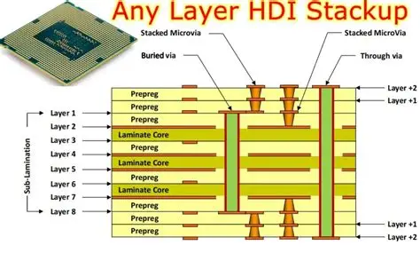
Common Types of PCB Markings
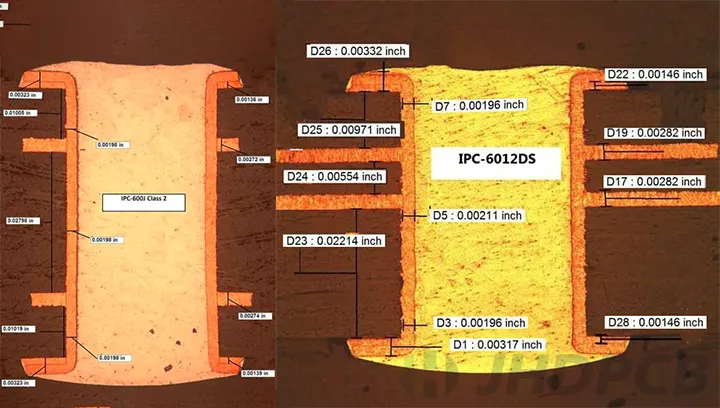
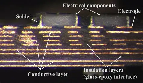
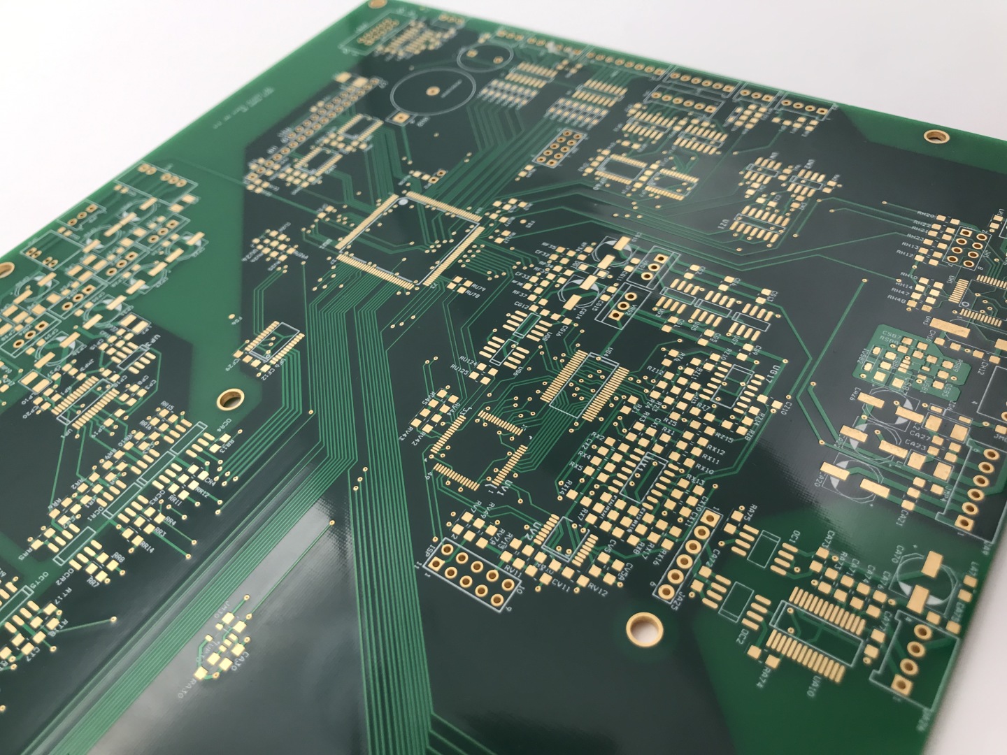
PCBs feature various markings etched, printed, or silkscreened onto panels or individual boards, serving as quick references for identification. Panel markings often include fabrication codes, date codes, and material specs, located along edges for easy inspection post-production. Component identification markings, like polarity indicators or pin numbers, aid assembly, while broader labels denote class levels per IPC standards. UL markings confirm safety testing, appearing as stylized logos with file numbers. Traceability codes link back to batches, crucial for troubleshooting failures in hobby projects. These elements collectively ensure boards meet performance expectations from design to deployment.
Silkscreen layers carry most user-facing info, using white or contrasting ink for readability. Factory-driven practices space markings to avoid interfering with traces or vias. Hobbyists benefit by scanning these for mismatches before populating boards. Common symbols include ground planes marked with chassis icons or test points labeled TP1. Misinterpreting them leads to assembly errors, so familiarity builds confidence in electronics basics.
Key Markings for Halogen-Free PCB Identification
The primary indicator for halogen-free PCBs is the "HF" marking, placed on the bare board or panel as per industry guidelines. This simple alphanumeric label confirms the base material lacks halogens, distinguishing it from standard laminates. Factories apply it during fabrication, often near the date code or material slash sheet notation. For hobbyists, spotting "HF" means the board suits low-toxicity applications without compromising solderability. Accompanying labels might reference laminate specs, but "HF" remains the direct halogen-free PCB identification cue. Always check multiple boards from a panel, as inner cuts may vary slightly.
Other symbols support this, like moisture sensitivity levels or finish types, but focus on base material for halogens. Green or specialized inks sometimes highlight eco-status, though text prevails for precision. In electronics basics, combining "HF" with IPC class markings verifies quality. Factories etch these durably to withstand cleaning and reflow, ensuring legibility post-assembly.
Standards Governing PCB Markings
Industry standards dictate marking placement, content, and durability to promote consistency across global supply chains. IPC/JEDEC J-STD-609 outlines requirements for symbols identifying halogen-free materials, mandating "HF" on qualifying boards. This ensures clear communication from factory to end-user, vital for hobbyist sourcing. IPC-4101 specifies base material qualifications, indirectly influencing marking needs for traceability. These documents emphasize external visibility without obscuring functionality. Adhering to them minimizes risks in mixed assemblies.
IPC-A-600 provides visual criteria for marking acceptability, covering legibility and adhesion across classes. Factories reference these during inspection, rejecting boards with faded or misplaced labels. For electronic hobbyists, standards demystify supplier claims, fostering reliable project outcomes.
Practical Best Practices for Reading PCB Markings
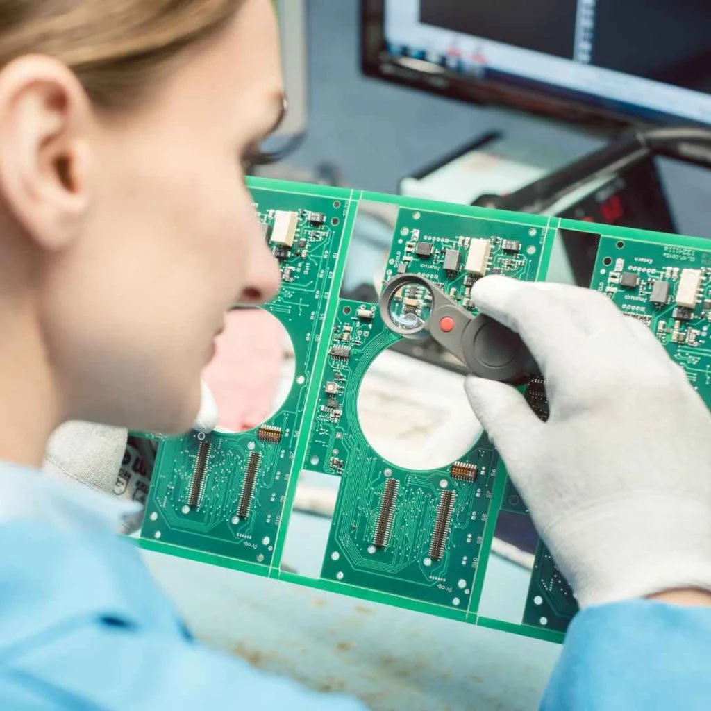
Start by examining the panel edges before routing individual boards, as comprehensive info resides there. Use a magnifying glass or loupe for fine print, noting "HF" alongside lot codes for full context. Cross-reference with datasheets if available, matching symbols to component identification needs. In soldering sessions, avoid heat damaging silkscreen, preserving markings for future reference. Clean boards gently post-inspection to maintain label integrity. These steps integrate factory insights into hobby workflows seamlessly.
For storage, label project bags with key markings photos, aiding inventory. Test continuity on marked test points early to validate layout. When ordering, specify halogen-free preferences, expecting "HF" confirmation. Troubleshooting starts here: unclear markings signal potential quality issues.
Related Reading: Halogen-Free PCBs: What Engineers Need to Know
Troubleshooting Misidentified or Missing Markings
Occasionally, markings fade from aggressive cleaning or handling, complicating halogen-free PCB identification. Verify via supplier docs or material tests if "HF" is absent but suspected. Component identification errors arise from similar symbols, so contextualize with board outline. Factory rejects ensure most reach users intact, but hobby mods risk erasure. Recreate critical labels with permanent markers if needed, noting originals. Persistent issues warrant batch checks for consistency.
In assemblies, mismatched markings cause reflow problems; always align with process capabilities. Electronics basics stress documentation: photo log every board. This proactive approach saves time in iterative prototyping.
Related Reading: Top 5 Misconceptions About Halogen Free PCB Manufacturing
Conclusion
Mastering PCB markings, especially for halogen-free boards, empowers hobbyists with professional-grade discernment. The "HF" symbol, backed by standards like IPC/JEDEC J-STD-609, simplifies identification amid diverse options. Common labels for materials, dates, and safety enhance project reliability and safety. Apply these insights to select, assemble, and troubleshoot effectively. As electronics evolve, this knowledge bridges hobby pursuits to sustainable practices. Equip your bench with this foundation for endless innovation.
FAQs
Q1: What does the "HF" marking mean on a PCB?
A1: The "HF" marking indicates halogen-free base materials, as defined in standards like IPC/JEDEC J-STD-609. It confirms low halogen content in laminates, aiding halogen-free PCB identification for safer electronics projects. Hobbyists check this for low-toxicity soldering and recycling. Placement is typically on panels or edges for easy spotting.
Q2: How can I tell if a PCB is halogen-free without markings?
A2: Rely on supplier certifications tied to IPC-4101 for material specs, as markings like "HF" are standard but not always visible post-routing. Request documentation confirming compliance during purchase. For electronics basics, this verifies environmental suitability without tests. Factory traceability ensures accuracy.
Q3: What are the most common PCB symbols for hobbyists?
A3: Key symbols include "HF" for halogen-free, UL for safety, and polarity marks for components. Date codes track age, while test points aid debugging. PCB markings like these support component identification and assembly. Understand them per IPC guidelines for reliable builds.
Q4: Why check PCB markings before assembly?
A4: Markings reveal material types, finishes, and compliance, preventing mismatches in reflow or compatibility. Halogen-free PCB identification via "HF" ensures safety in home setups. This factory-driven practice minimizes rework. Integrate into your workflow for smoother electronics basics.