 ALLPCB


Introduction
RF laminate PCB materials form the foundation for high-frequency circuits in applications ranging from telecommunications to radar systems. These specialized substrates must maintain signal integrity at gigahertz frequencies where standard materials falter. Electrical engineers selecting RF PCB material properties prioritize dielectric constant, loss tangent, and thermal conductivity to minimize losses and ensure stability. This article explores these critical attributes, comparing options like PTFE-based laminates against conventional FR4. Understanding these properties enables precise impedance control and reliable performance in demanding environments. By aligning material choice with design goals, engineers unlock superior RF system efficiency.
What Are RF Laminate PCB Materials and Why Do They Matter?
RF laminate PCB materials consist of dielectric substrates reinforced for microwave and millimeter-wave operations. Unlike general-purpose laminates, they exhibit controlled electrical characteristics to support propagation with minimal distortion. The dielectric constant RF PCB value dictates signal velocity and line dimensions, while low loss tangent preserves amplitude over distance. In high-speed designs, thermal conductivity RF laminate performance prevents hotspots that degrade reliability. These materials adhere to specifications like IPC-4101, ensuring consistency in multilayer constructions. Their relevance grows with 5G, satellite communications, and automotive radar, where signal attenuation directly impacts range and data rates.
Engineers face trade-offs in mechanical stability, cost, and processability when specifying RF laminates. Standard FR4 suffices for lower frequencies but introduces excessive losses above a few gigahertz due to higher dissipation. Specialized RF laminates, often ceramic-filled or woven-glass reinforced, balance electrical excellence with manufacturability. Industry standards such as IPC-TM-650 method 2.5.5.5 provide standardized testing for dielectric properties, allowing direct comparisons. Selecting the right material optimizes board size, power handling, and thermal management. Ultimately, RF PCB material properties determine whether a design meets performance margins in real-world deployments.
Key RF PCB Material Properties Explained
Dielectric Constant in RF PCBs
The dielectric constant, or Dk, quantifies a material's ability to store electrical energy relative to air. In RF PCB material properties, lower and stable Dk values enable faster signal propagation and compact trace widths for controlled impedance. Typical FR4 offers Dk around 4.0 to 4.8 at 1 GHz, but this varies with frequency and temperature, complicating high-speed simulations. RF laminates achieve Dk from 2.1 to 3.5, remaining consistent up to 40 GHz due to non-polar structures. This stability reduces phase shifts and crosstalk in multilayer stacks. Engineers measure Dk using stripline or cavity resonators per established test methods to validate supplier data.
Frequency dependence proves critical; resin-based materials see Dk rise at higher bands, while advanced RF options hold steady. Temperature coefficients also matter, as excursions alter effective Dk and mismatch with copper. Ceramic-filled variants slightly elevate Dk for better mechanical properties without sacrificing uniformity. In practice, a Dk tolerance of ±0.05 across a panel ensures repeatable impedance. Designers simulate with nominal values but verify prototypes to account for anisotropy in z-axis versus xy-plane. Precise Dk control directly enhances filter performance and antenna efficiency.
Loss Tangent and Signal Attenuation
Loss tangent, or Df, measures dielectric energy converted to heat, directly scaling insertion loss in transmission lines. For dielectric constant RF PCB and loss tangent RF PCB combinations, low Df below 0.005 at 10 GHz minimizes attenuation in long traces or antennas. FR4 typically shows Df of 0.02, acceptable up to 2 GHz but punitive at millimeter waves. RF laminates deliver Df from 0.0001 to 0.002, preserving signal strength for power-critical applications. This property compounds with conductor losses, so material selection halves total path attenuation in many cases.
Df exhibits mild frequency upturn, but RF materials maintain superiority over broad spectra. Moisture absorption exacerbates losses in hydrophilic substrates, underscoring the need for low water uptake. Testing per IPC-TM-650 captures Df accurately, guiding qualification. In stacked dielectrics, average Df dictates overall performance, favoring uniform laminates. Engineers budget Df in link analysis to meet noise figures. Lower loss tangent RF PCB values thus extend operational range without amplifiers.
Thermal Conductivity and Reliability
Thermal conductivity RF laminate quantifies heat spreading from active components to sinks. RF materials range from 0.3 to 1.0 W/mK, outperforming FR4's 0.3-0.5 W/mK through fillers like ceramics. Higher values prevent localized heating that shifts Dk or accelerates aging. In power amplifiers, efficient dissipation maintains gain flatness across bands. CTE matching to copper foil averts warpage during reflow or cycling. Z-axis conductivity aids via reliability under thermal stress.
Multilayer boards amplify thermal gradients, making conductivity paramount for IPC-6012 compliance. Engineers model junctions with material datasheets to predict hotspots. Enhanced thermal conductivity RF laminate supports higher power densities in phased arrays. Vias and planes augment in-plane spreading, but substrate sets the baseline. Reliability testing simulates field conditions, confirming margins.
Related Reading: RF PCB Design: Challenges and Solutions for High-Frequency Applications
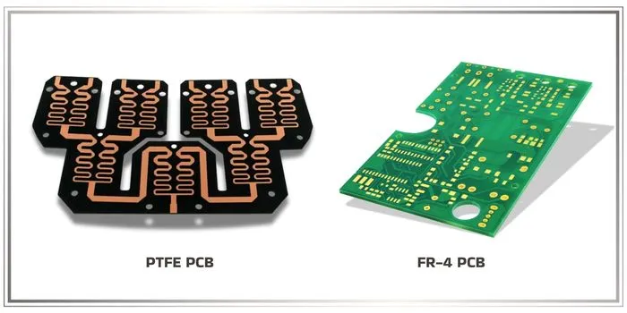
PTFE vs FR4 for RF PCB Applications
PTFE-based laminates excel in RF due to inherently low Dk of 2.1-2.6 and Df under 0.002, far surpassing FR4. PTFE vs FR4 RF PCB comparisons highlight PTFE's frequency-stable properties, ideal for broadband circuits. FR4 processes easily with standard drills and plating, suiting prototypes or low-GHz boards. PTFE demands specialized techniques like sodium etching for adhesion, increasing lead times and costs. Mechanical rigidity favors FR4 for rigid-flex hybrids, while PTFE suits pure high-frequency purity.
Thermal conductivity RF laminate edges to filled PTFE at 0.5-1.0 W/mK versus FR4's modest rating, aiding dense layouts. CTE mismatch in pure PTFE requires hybrids with glass or ceramics for via integrity. FR4's higher Tg limits it to moderate temperatures, whereas PTFE handles extremes. Loss tangent RF PCB dominance makes PTFE mandatory above 10 GHz, but FR4 prototypes validate concepts economically. Designers hybridize cores for cost-performance balance. In summary, PTFE unlocks peak RF potential where FR4 introduces compromises.
Related Reading: PTFE PCBs for Medical Devices: Ensuring Reliability and Performance
Best Practices for Selecting and Implementing RF Laminates
Start with frequency and loss budget to narrow RF PCB material properties. Simulate impedance with vendor models, targeting 50-ohm lines. Specify Dk/Df at operating frequency and temperature for accuracy. Prototype on hybrid stacks blending PTFE cores with FR4 outer layers for machinability. Qualify per IPC standards, measuring warpage and peel strength post-lam. Control stackup symmetry to minimize bow.
Fabrication tolerances tighten for RF: ±10% dielectric thickness, low roughness copper. Bake boards to desorb moisture before assembly. Thermal vias and ground planes enhance conductivity. Field-tune filters post-assembly for material variations. Document properties in design files for iterations. These steps ensure production yields align with simulations.
Conclusion
RF laminate PCB materials elevate performance through optimized dielectric constant RF PCB, loss tangent RF PCB, and thermal conductivity RF laminate traits. PTFE outperforms FR4 in high-frequency regimes, trading processability for superior signal fidelity. Engineers benefit from structured selection, leveraging standards for reproducibility. Balancing properties yields compact, reliable boards for next-generation RF systems. Prioritizing these factors unlocks efficiency in evolving applications.
FAQs
Q1: What role does dielectric constant RF PCB play in impedance control?
A1: Dielectric constant RF PCB determines signal velocity and trace width for 50-ohm lines. Lower, stable Dk around 2.1-3.5 reduces size while minimizing variations. Frequency and temperature stability prevents phase errors in filters. Verify with test coupons per standard methods during qualification. This ensures simulation-to-hardware correlation in RF designs.
Q2: How does loss tangent RF PCB affect high-frequency attenuation?
A2: Loss tangent RF PCB quantifies dielectric heating, scaling insertion loss linearly. Values below 0.002 preserve amplitude in mmWave traces versus higher Df materials. It compounds with skin effect, so low Df extends range. Measure at band center for accuracy. Optimal selection halves path losses in amplifiers.
Q3: Why prioritize thermal conductivity RF laminate in power RF boards?
A3: Thermal conductivity RF laminate spreads heat from GaN devices, stabilizing Dk and averting failures. Rates above 0.5 W/mK outperform basics, supporting dense arrays. Pair with vias for z-axis relief. It maintains performance under load per reliability specs. Critical for phased arrays and radars. (54 words)
Q4: In PTFE vs FR4 RF PCB, when to choose each?
A4: PTFE vs FR4 RF PCB favors PTFE for GHz+ with ultra-low Dk/Df, despite processing challenges. FR4 suits sub-5 GHz prototypes economically. Hybrids combine strengths for multilayers. Assess loss budget and budget first. Standards guide qualification for both.
References
IPC-4101E - Specification for Base Materials for Rigid and Multilayer Printed Boards. IPC, 2017
IPC-TM-650 2.5.5.5 - Dielectric Constant, Dissipation Factor and Loss Tangent. IPC, 2018
IPC-6012E - Qualification and Performance Specification for Rigid Printed Boards. IPC, 2017
IPC-6018DS - Qualification and Performance Specification for High Frequency (Microwave) Printed Boards. IPC, 2020


